In today’s educational environment, technology plays a key role in enhancing teaching and learning experiences. PRIMA’s All-in-One Interactive Flat Panel (IFP) integrates powerful features, offering a seamless solution for modern classrooms.


Key Features for Classroom Success


🔹Interactive Touch & Collaboration:
The IFP enables real-time interaction with content, making lessons more engaging. Multiple students can collaborate on the screen, promoting teamwork and learning.

🔹Multi-Screen Grouping & Sharing:

Multiple IFPs can be grouped to display synchronized content, facilitating group work and ensuring all students see the same information.

🔹IoT Control:

The IFP integrates IoT control, allowing seamless management of connected devices, enhancing classroom efficiency and streamlining operations.

🔹Smart Whiteboard:

Built-in smart whiteboard capabilities enable instant annotation and saving of content, making lessons more dynamic and flexible.


How PRIMA IFP Benefits the Classroom


🔹High Cost Performance:

One IFP can realize  the smart classroom solution.

🔹Various Usage Scenarios:

Perfect for collaborative classrooms, but also for standalone use on a single device

🔹 Enhanced Engagement:

Students actively participate with interactive tools, improving engagement and retention.


PRIMA’s All-in-One Interactive Flat Panel redefines the classroom by merging interactive, collaborative, and educational technology into one device. It empowers teachers, engages students, and fosters an efficient and smart learning environment.

The Z178 Smart Watch redefines what a wearable device can do, blending style and functionality into one sleek package. With its stunning HD Retina display and IP68 waterproof rating, this watch is built to keep up with your active lifestyle while maintaining a premium look. Whether you're swimming, running, or attending a business meeting, the Z178 adapts effortlessly to your needs while providing crystal-clear visibility in any lighting condition.


Beyond its elegant design, the Z178 excels in keeping you connected and healthy. The built-in Bluetooth calling feature allows you to take calls directly from your wrist, while real-time notifications ensure you never miss important messages. Fitness enthusiasts will appreciate the 123+ sports modes and advanced tracking capabilities that monitor everything from steps to calories burned. The watch even reminds you to stay hydrated, making it a true wellness partner that cares about your daily habits.


What truly sets the Z178 apart is its ability to match your personal style. With hundreds of customizable watch faces, you can switch between sporty, classic, or modern designs to suit any occasion. Combined with long battery life and durable construction, this smartwatch is more than just a gadget—it's a reliable companion for every adventure. Whether you're exploring the outdoors or navigating a busy workday, the Z178 is designed to enhance your life with smart technology and timeless style.


How to Choose Between RO4350B, PTFE, and Ceramic-Filled Substrates?


Introduction

High-frequency PCBs are critical in modern RF and microwave applications, including 5G communications, radar systems, and satellite technology. Selecting the right substrate material is essential to ensure signal integrity, thermal stability, and manufacturability. Three of the most commonly used high-frequency PCB materials are Rogers RO4350B, PTFE (Teflon), and ceramic-filled laminates.


In this guide, we’ll explore the properties, advantages, and trade-offs of each material and provide insights on how to choose the best option for your application. We’ll also showcase a real-world6-layer RF PCB example using RO4350B and RO4450F bondply to illustrate material selection in practice.


Key Considerations for High-Frequency PCB Materials

Before diving into material specifics, let’s outline the key factors that influence substrate selection:


  • -Dielectric Constant (Dk)–Affects signal propagation speed and impedance control.
  • -Dissipation Factor (Df)–Determines signal loss at high frequencies.
  • -Thermal Conductivity–Important for heat dissipation in power applications.
  • -Coefficient of Thermal Expansion (CTE)–Impacts reliability under thermal cycling.
  • -Manufacturability–Some materials require specialized processing.
  • -Cost- High-performance materials can be expensive.


Now, let’s compare the three leading high-frequency PCB materials.


1. RO4350B: The Cost-Effective High-Performance Option

Rogers 4350B is a woven glass-reinforced hydrocarbon/ceramic laminate that offers a balance between electrical performance and ease of fabrication.


Key Features of RO4350B


  • -Dielectric Constant (Dk): 3.48±0.05 @ 10 GHz
  • -Dissipation Factor (Df): 0.0037 @ 10 GHz (low loss)
  • -Thermal Conductivity: 0.69 W/m/°K (better than FR4)
  • -CTE: Low expansion (X/Y: 10-12 ppm/°C, Z: 32 ppm/°C)
  • -Tg (Glass Transition Temp): >280°C (excellent thermal stability)
  • -Moisture Absorption: 0.06% (minimal impact on performance)


Why Choose RO4350B?

✔Cost-Effective Alternative to PTFE–RO4350B performs close to PTFE but at a lower cost.

✔Compatible with Standard FR4 Processes–No special drilling or plating required.

✔Stable Dk Over Frequency & Temperature–Ideal for RF and microwave circuits.

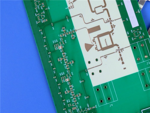
6-Layer RO4350B PCB 1.8mm Thick


Example: 6-Layer RF PCB Using RO4350B

Here’s a real-world PCB we manufactured using RO4350B cores and RO4450F bondply:


Layer Count: 6

Dimensions: 98.5 mm×68 mm (±0.15mm)

Min Trace/Space: 4/6 mils

Min Hole Size: 0.3mm

Blind Vias: L1-L2, L3-L6, L5-L6

Board Thickness: 1.8mm

Surface Finish: Immersion Gold

Solder Mask: Green (top & bottom)

Quality Standard: IPC-Class-2


Stackup Structure:


Top Layer (35µm Cu)

RO4350B Core (0.254mm)

Inner Layer (35µm Cu)

RO4450F Bondply (4mil, 2x)

RO4350B Core (0.762mm)

Bottom Layer (35µm Cu)


This design is optimized for RF applications with controlled impedance and low insertion loss.


2. PTFE (Teflon): The Ultra-Low Loss Solution

PTFE (Polytetrafluoroethylene) is the gold standard forultra-high-frequency PCBs due to its extremely low loss.


Key Features of PTFE


  • Dk: 2.1–3.5 (varies with filler material)
  • Df: As low as 0.0009 (best for mmWave applications)
  • Thermal Stability: Excellent, but high CTE (~160 ppm/°C)
  • Challenges: Requires specialized drilling/plating processes.


When to Use PTFE?

✔Millimeter-Wave (mmWave) Circuits (24GHz+, 5G, radar)

✔Extremely Low-Loss Applications (satellite comms, aerospace)

✖Not Ideal for Cost-Sensitive Projects (higher fabrication costs)


3. Ceramic-Filled Materials: High Thermal & Mechanical Stability

Ceramic-filled substrates (e.g.,Rogers RO3000 series) offer enhanced thermal conductivity and mechanical strength.


Key Features of Ceramic-Filled Laminates


  • Dk: 3.0–10.2 (adjustable based on ceramic content)
  • Df: 0.001–0.003 (low loss, but not as good as PTFE)
  • Thermal Conductivity: Up to 4 W/m/°K (great for power amplifiers)
  • CTE: Matches copper (~17 ppm/°C), reducing warping risks.


Best Applications for Ceramic-Filled PCBs

✔High-Power RF Devices (base stations, power amplifiers)

✔Applications Needing Heat Dissipation (automotive radar, LED PCBs)


Material Selection Guide: RO4350B vs. PTFE vs. Ceramic


Parameter

RO4350B

PTFE

Ceramic-Filled

Dk (10 GHz)

3.48 ±0.05

2.1–3.5

3.0–10.2

Df (10 GHz)

0.0037

0.0009–0.002

0.001–0.003

Thermal Conductivity

0.69 W/m/°K

Low (~0.2)

Up to 4 W/m/°K

CTE (ppm/°C)

X/Y: 10-12, Z: 32

~160 (high)

~17 (matches Cu)

Cost

Medium

High

Medium-High

Manufacturing Ease

Easy (FR4-like)

Difficult (special processes)

Moderate


Which One Should You Choose?


  • For most RF applications (up to 20GHz), RO4350B Frequency PCB is the best balance of cost and performance.
  • For mmWave (24GHz+), PTFE is ideal but expensive.
  • For high-power/high-thermal applications, ceramic-filled laminates are superior.


Conclusion

Selecting the right high-frequency PCB material depends on your application’s frequency range, thermal requirements, and budget.

RO4350B PCB is the best all-around choice for most RF designs, offering low loss, stable Dk, and easy fabrication.


PTFE is unmatched for ultra-low-loss mmWave circuits but comes at a higher cost.


Ceramic-filled materials excel in high-power and high-thermal scenarios.


Our 6-layer RF PCB example demonstrates howRogers4350B and RO4450F bondply can be used effectively in real-world designs. If you need high-frequency PCBs with optimized material selection, we provide global manufacturing with IPC-Class-2 quality standards.


Need a custom RF PCB solution? Contact us today for expert guidance!


PTFE Materials Are Difficult to Process—How to Solve Lamination and Drilling Challenges?


Introduction

Polytetrafluoroethylene (PTFE), commonly known by the brand name Teflon (TFE), is a high-performance material widely used in printed circuit boards (PCBs) for high-frequency applications. Its low dielectric constant (Dk) and dissipation factor (Df) make it ideal for RF, microwave, and millimeter-wave circuits. However, TFE materials like Rogers RT/duroid 5880 present significant challenges in lamination and drilling due to their unique properties.


In this article, we’ll explore the key difficulties in TFE material PCB fabrication and provide practical solutions to overcome them. We’ll also highlight how our 3-layer rigid PCB with RTduroid 5880 and RO4450F bonding ply successfully addresses these challenges while maintaining high-frequency performance.


Why TFE Materials Are Difficult to Process

PTFE-based laminates like RT/duroid 5880 offer outstanding electrical properties, including:


  • -Low dielectric constant (Dk = 2.2±0.02)
  • -Ultra-low dissipation factor (Df = 0.0009 at 10 GHz)
  • -Excellent thermal stability


However, these benefits come with manufacturing challenges:


1. Lamination Difficulties


  • -Poor Adhesion: PTFE is inherently non-sticky, making it difficult to bond with copper layers.
  • -Thermal Expansion Mismatch: PTFE has a higher coefficient of thermal expansion (CTE) than copper, leading to potential delamination.
  • -Resin Flow Control: Excessive heat and pressure can cause resin squeeze-out, affecting dielectric thickness.


2. Drilling Challenges


  • -Material Softness: PTFE is soft and prone to smearing during drilling, leading to poor via quality.
  • -Thermal Sensitivity:Excessive heat from drilling can degrade PTFE’s electrical properties.
  • -Hole Wall Roughness: Improper drilling can result in rough via walls, affecting signal integrity.


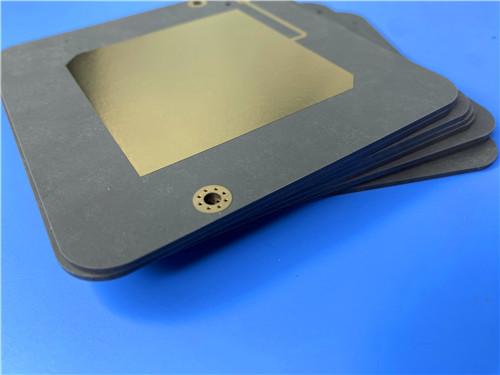
RTduroid 5880 PCB 3-layer 3.3mm Thick Immersion Gold


Solutions for Successful TFE PCB Fabrication


1. Optimizing Lamination for TFE Materials

a) Use Special Bonding Materials

To improve adhesion, we use RO4450F bonding ply—a thermoset material compatible withPTFE laminates. In our 3-layer PCB stackup, RO4450F ensures strong interlayer bonding while maintaining electrical performance.


Our PCB Stackup Example:


Layer 1: Copper (35μm)

Core: RT/duroid 5880 (1.575 mm)

Layer 2: Copper (35μm)

Bonding Ply: RO4450F (0.102 mm)

Core: RT/duroid 5880 (1.575 mm)

Layer 3: Copper (35μm)


b) Controlled Lamination Parameters


  • Temperature & Pressure: Precise control prevents resin flow issues and maintains consistent dielectric thickness.
  • Slow Ramp-Up Rates: Gradual heating minimizes thermal stress, reducing delamination risks.


2. Overcoming Drilling Challenges

a) Specialized Drill Bits & Parameters


  • Carbide Drill Bits: Harder than standard drills, reducing PTFE smearing.
  • Optimized RPM & Feed Rate: Prevents excessive heat buildup.


b) Laser Drilling for Micro-Vias


  • For smaller holes (0.4mm in our PCB), laser drilling provides cleaner, more precise vias with minimal wall roughness.


c) Post-Drilling Treatments


  • Plasma Etching: Removes PTFE residue from via walls.
  • Via Plating (20μm in our PCB): Ensures reliable electrical connections.


Case Study: Our 3-Layer RT/duroid 5880 PCB

To demonstrate successful TFE material processing, here’s a breakdown of our high-frequency PCB solution:


Key Specifications:

Material: RT/duroid 5880 (core) + RO4450F (bonding ply)

Layers: 3

Board Thickness: 3.3 mm

Min Trace/Space: 5/7 mils

Min Hole Size: 0.4 mm

Via Plating Thickness: 20μm

Surface Finish: Immersion Gold (enhances signal integrity)


Why This Design Works for High-Frequency Applications?

✔Low Signal Loss: RT/duroid 5880’s ultra-low Df ensures minimal RF attenuation.

✔Stable Dk: Uniform dielectric constant across frequencies.

✔Robust Construction: RO4450F bonding ply prevents delamination.

✔Precision Drilling: 0.4mm vias with 20μm plating ensure reliable interconnects.


Conclusion: Partner with a PCB Supplier Experienced in TFE Materials

Fabricating High Frequency PTFE PCB with RT/duroid 5880 and other PTFE-based materials requires specialized expertise in lamination, drilling, and thermal management. By optimizing bonding materials, drilling techniques, and lamination processes, we deliver high-performance PCBs for RF, aerospace, and millimeter-wave applications.


Looking for a reliable TFE PCB supplier? Our 3 Layer High Frequency PCB RT/duroid 5880 is IPC-Class-2 compliant, electrically tested, and available worldwide. Contact us today for high-frequency PCB solutions tailored to your needs!


What Are the Design Considerations for Hybrid High-Frequency PCBs?


Introduction

Hybrid (mixed dielectric) high-frequency PCBs combine different materials to optimize electrical performance, thermal stability, and manufacturability. These mixed dielectric hybrid boards are widely used in RF/microwave applications, aerospace, radar systems, and telecommunications, where signal integrity and thermal management are critical.


Designing hybrid PCB requires careful consideration of material properties, layer stackup, signal integrity, and manufacturing constraints. In this article, we explore key design considerations and provide practical insights, using a 4-layer hybrid PCB (RO4350B + High-Tg FR-4 S1000-2M) as an example.


1. Material Selection and Compatibility

Key Factors in Material Selection


Dielectric Constant (Dk) & Loss Tangent (Df):


  • -High-frequency signals require stable Dk and low-loss materials (e.g., Rogers RO4350B with Dk=3.48, Df=0.0037).
  • -FR-4 (S1000-2M) provides mechanical support but has higher loss, so it’s best used in non-critical layers.


Thermal Expansion (CTE) Mismatch:


  • -RO4350B has a CTE close to copper (X/Y: 10-12 ppm/°C), reducing warpage and via reliability issues.
  • -S1000-2M offers excellent Z-axis CTE for plated through-hole (PTH) reliability.


Thermal Conductivity & Tg:


  • -RO4350B has a high Tg (>280°C) and thermal conductivity (0.69 W/m/°K), making it suitable for high-power RF designs.
  • -S1000-2M (Tg 180°C) provides mechanical stability and lead-free compatibility.


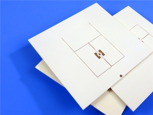
4-Layer Hybrid PCB 10mil RO4350B and High Tg FR-4


Example PCB Construction

Our 4-layer hybrid circuit board combines:


Signal Layers (RO4350B): Optimized for RF performance.

Core/Prepreg (FR-4 S1000-2M): Provides structural integrity.


Stackup:

Layer 1 (RF Signal): 35μm Cu + RO4350B (0.254mm)

Layer 2 (Ground/Power): 35μm Cu + Prepreg (0.254mm)

Layer 3 (Inner Signal): 35μm Cu + S1000-2M (0.8mm)

Layer 4 (Bottom Layer): 35μm Cu


2. Signal Integrity and Impedance Control

Critical Design Rules


Controlled Impedance Routing:


  • RO4350B’s stable Dk allows precise impedance matching (e.g., 50Ωmicrostrip lines).
  • Use field solvers to calculate trace width/spacing (e.g., 4/6 mil traces in our example).


Minimizing Crosstalk & Loss:


  • Keep high-speed traces short and avoid sharp bends.
  • Use ground planes (Layer 2 in our stackup) to reduce interference.


Via Optimization:


  • Our example Hybrid PCB Board PCB uses 0.20mm minimum hole size with 20μm plating thickness for reliability.
  • Avoid blind vias to simplify manufacturing (as seen in our design).


3.Thermal Management Considerations


Preventing Delamination & Warpage


  • CTE Matching: RO4350B’s low CTE reduces stress between layers.
  • Thermal Relief in Pads: Prevents excessive heat during soldering.


Heat Dissipation Strategies


  • Copper Weight: Our PCB uses 1oz (35μm) copper for balanced current handling and heat spreading.
  • Surface Finish: ENIG (Electroless Nickel Immersion Gold) ensures reliable solderability and corrosion resistance.


4. Manufacturing and Reliability

Fabrication Tolerances


  • Board Dimensions: 173mm x 85.3mm (±0.15mm tolerance).
  • Solder Mask & Silkscreen: Green solder mask (top/bottom) with white/green silkscreen for component marking.


Quality Assurance


  • 100% Electrical Testing: Ensures no short/open circuits before shipment.
  • IPC-Class-2 Compliance: Guarantees reliability for commercial applications.


5. Applications of Hybrid High-Frequency PCBs

Our example PCB (RO4350B + S1000-2M) is ideal for:

✅Radar & Guidance Systems (stable Dk, low loss)

✅5G & Millimeter-Wave Antennas (precise impedance control)

✅Aerospace & Defense Electronics (high thermal reliability)


Conclusion

Designing hybrid high-frequency PCBs requires a balance between material properties, signal integrity, and manufacturability. By selecting compatible materials (like RO4350B FR-4 hybrid PCB), optimizing stackup, and following best practices in impedance control and thermal management, engineers can achieve high-performance RF/microwave designs.


Looking for a reliable hybrid PCB supplier? Our 4-layer mixed-dielectric PCB (RO4350B + S1000-2M) meets stringent RF and thermal requirements while ensuring cost-effective production. Contact us today for your high-frequency PCB needs!


In recent years, with the continuous development of RFID technology, the application of RFID has become more and more extensive, reaching every aspect of people's daily lives.

RFID technology is known as one of the most promising technologies in the 21st century.


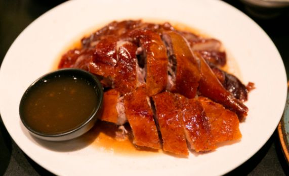
According to statistics, about 700 million goose meat is consumed in the country every year, of which at least 170 million goose is consumed in Guangdong Province. The reason why Guangdong can eat a lot of geese every year is inseparable from the traditional local dish: Cantonese roast goose

The production process of Cantonese-style roast goose is extremely complicated. From material selection to roasting, it involves more than 20 production processes, and more than a dozen kinds of roast goose fillings are matched and made. Any step will affect the taste of roast goose. D & H SMARTID Co., Ltd. has been committed to supporting solutions for embedded applications in the RFID industry, and has the ability to integrate production + R&D + solutions into the Internet of Things. Applying RFID technology to the tracking of food processing is a set of solutions customized according to customer needs.

A well-known roast goose chain brand in Dongguan, Guangdong took the lead in applying RFID technology to the production process of roast goose. Before roasting goose is roasted in the oven, each goose needs to go through more than 20 pretreatment processes. How to ensure the integrity of the pretreatment process is the key to achieving deliciousness.

In the pretreatment process of roasting goose, an RFID tag is added to each goose to be processed, which is equivalent to an ID card and is used to record processing information. After each process, the information is written into the RFID tag to ensure that each goose can complete each pretreatment process to ensure that each roast goose has the same delicious taste.

Apply RFID technology to product identification in the production process of various industries to ensure production quality and production efficiency analysis, and to improve the manufacturing process to increase efficiency, reduce costs, and increase benefits.

RFID technology has attracted much attention due to its long-distance reading, high storage capacity, small size, diversified shapes, anti-pollution ability and durability. It is the future of Internet of Things applications and industrial manufacturing 4.0 (intelligent manufacturing, logistics, The key technologies of healthcare, agriculture, and food supply chain will inevitably develop in a diversified direction.

The application of RFID technology to the production process of roast goose is a manifestation of the diversified development and application of RFID technology. The use of high-temperature resistant RFID tags made of food-grade PET materials to realize the full traceability of the production and processing process of roast goose, ensuring the taste of Cantonese cuisine, and making the production process more and more standardized.


RFID antenna is one of the necessary hardware for the application of RFID technology. With the rapid development of RFID technology, RFID antenna has also been developed rapidly. The goal of the antenna is to transmit the maximum energy in and out of the chip. How to match the design of the antenna with the free space and the tag chip connected to it is a factor restricting the development of the antenna.

The design and manufacture of RFID tag antennas are affected by application restrictions, the shape and physical characteristics of the objects identified by the antenna characteristics, as well as the objects around the antenna and the environment. This is an important aspect of RFID technology research in the diversified development of RFID technology applications. direction.

With the progress and development of RFID technology, more and more new RFID products have been manufactured and are well applied. In the future, the development of RFID electronic tags will also tend to be green and diversified in raw materials to meet the application needs of different industries.

With the rapid development of technology, RFID (Radio Frequency Identification) technology has gradually penetrated into various fields of our lives. As an important application tool of RFID technology, RFID handheld devices are playing an increasingly important role in various industries due to their high efficiency, accuracy, and convenience. This article will delve into and analyze the application of RFID handheld devices in various industry inventories.

1 Overview of RFID Handheld Phone Technology

RFID technology is a wireless communication technology that identifies specific targets through radio signals and reads and writes relevant data. RFID handheld devices are PDAs (portable mobile terminals) that combine RFID technology with portable mobile hardware and have specific functions such as RFID reading and writing. RFID handheld devices have the characteristics of small size, light weight, and long service life, which can quickly and accurately extract and write information.

2 The application of RFID handheld devices in various industry inventories

1. Retail industry

In the retail industry, RFID handheld devices are a powerful assistant for inventory management and inventory. By attaching RFID tags to products and using RFID handheld devices for scanning, retailers can update inventory data in real-time, ensuring the accuracy of inventory information. In addition, RFID handheld devices can help retailers conduct rapid inventory, reduce labor and time costs, and improve operational efficiency.

2. Manufacturing industry

In the manufacturing industry, RFID handheld devices play an important role in production process control and asset management. By applying RFID tags to components and equipment on production lines, manufacturers can use RFID handheld devices to track production progress in real-time and optimize production processes. Meanwhile, RFID handheld devices can also be used for asset management of devices, ensuring accurate location and maintenance records, improving device utilization and lifespan.

3. Logistics and Supply Chain Management

In the fields of logistics and supply chain management, RFID handheld devices are key tools for tracking and managing goods. By attaching RFID tags to goods and using RFID handheld devices for scanning, logistics companies can real-time understand the location and status of goods in the supply chain, achieving full process visualization of goods. This helps enterprises optimize transportation and logistics processes, improve transportation efficiency and customer satisfaction.

4. Library management

The traditional book inventory method requires scanning and recording book information one by one, which is very time-consuming and cumbersome. By using RFID technology, multiple tag information can be read simultaneously by simply approaching the storage location of the scanned book with an RFID handheld terminal, greatly improving the inventory speed. By pasting an RFID tag on each book as a unique identification. The use of RFID handheld terminals allows for quick and accurate counting within the museum, achieving fast speed and high accuracy.

5. Asset management

In enterprise fixed asset management, RFID handheld devices are used for asset inventory and tracking management. RFID handheld devices have powerful tag group reading capabilities, which can quickly read and identify RFID tags on each asset, and match them with information in the database, improving the efficiency and accuracy of inventory work. In addition, by attaching RFID tags to assets, enterprises can use RFID handheld devices to quickly and accurately obtain information on the location, usage status, and other information of assets. This helps enterprises to have real-time understanding of asset status, improve asset utilization and management efficiency.

6. Warehouse management

Compared to traditional inventory methods, RFID handheld terminals have significantly improved work efficiency. Warehouse administrators can easily scan item labels with an RFID handheld device to complete inventory work, eliminating the need to scan barcodes one by one or perform manual counting. By scanning the RFID tags on the goods, the handheld device can quickly read the information of the goods, such as quantity, type, batch, etc., and update it in real-time to the warehouse management system. This not only reduces the time and error rate of manual inventory, but also enables real-time inventory monitoring and early warning, improving the intelligence level of warehouse management.

3 Industry Case Study

Taking a clothing retail enterprise as an example, it uses RFID handheld devices for inventory counting and product tracking. By attaching RFID tags to each item and using RFID handheld devices for scanning and recording, enterprises have achieved real-time monitoring and rapid inventory of product inventory. At the same time, RFID handheld devices can also synchronize data with the backend system in real-time, ensuring the accuracy and timeliness of inventory data. This management method greatly improves the efficiency and accuracy of inventory management, and reduces the risk of goods loss.

With the rapid development of information technology and the advancement of smart city construction, RFID smart bookcases, as an emerging intelligent management tool, have received increasing attention and favor from libraries, schools, enterprises, and public service institutions. So, how big is the domestic RFID smart bookshelf market? This article will provide you with an in-depth analysis of the demand, scale, and prospects of this market. As the channels for obtaining real data are limited, the market forecast data and calculation results in this article are for reference only.

Market demand for RFID smart bookcases

Library and Education Sector

University Library: University libraries manage a large number of books and literature materials. RFID smart bookcases can greatly improve the efficiency of book borrowing and returning, reduce manual operations, lower management costs, and enhance the user experience for teachers and students. At the same time, smart bookcases can achieve precise inventory and quick positioning, improving management efficiency.

Public Library: As an important place for social education, public libraries need to meet the needs of a wide range of readers. The self-service borrowing and returning function of RFID smart bookcases can not only reduce readers' waiting time and improve service quality, but also help libraries achieve efficient book management and reduce manual workload.

Primary and secondary school libraries: Primary and secondary school libraries are important places for students to acquire knowledge. The introduction of RFID smart bookcases not only facilitates students' self-service borrowing and returning of books, but also cultivates their reading habits and information literacy, providing schools with intelligent management tools.

Enterprise and Public Services

Internal management of enterprises: In large enterprises and research institutions, RFID smart bookcases can be used to manage internal books and materials, achieving efficient knowledge management and data archiving. Enterprise employees can quickly find the necessary information and improve work efficiency through the self-service borrowing and returning system.

Community service: In the construction of smart cities, the intelligent transformation of community bookshelves has become an important component. RFID smart bookcases can not only provide convenient reading services for community residents, but also achieve cross regional book resource sharing through networking, improving book utilization.

Market size calculation of RFID smart bookshelf

Global RFID Market Size

According to market research reports, the global RFID market is expected to reach a size of $16.4 billion in 2023 and grow at a compound annual growth rate (CAGR) of around 10%. It is projected to reach $18.04 billion by 2024.

Java Card is a microprocessor-based smart card, which consists of multiple elements: hardware, Java Card operating system, security module (card manager) and one or more Applets at the time of release.


Hardware

There are various hardware manufacturers, but, it should be noted that the most popular are NXP and Infineon. The two silicon manufacturers ship millions of microprocessor chips worldwide each year. They have been certified by EMVCo, Visa, MasterCard and UnionPay International to provide you with a hardware platform with first-class security.


operating system

Java Smart Card OS is an operating platform that utilizes hardware functions and allows applications (small programs) written in the Java programming language to run on the card. Java Card is an open platform, and its standards (and development kits) are available for free from Oracle’s Java website.


Card manager

One of the main functions of the microprocessor card is its security function. A separate area of the chip is designated specifically for this purpose, the “card manager”. This is an application that permanently resides on the chip, has the function of performing card and applet management, and is a gateway to a security element (called a security domain). This central component is defined by another open platform standard GlobalPlatform.


GlobalPlatform (globalplatform.org) is an independent standards body run by its members. Members include Apple, Oracle, Samsung, American Express, Gemalto, NXP, HID, Visa, Infineon, MasterCard, etc.


Applets

An applet is a program that runs on the card that the user (or terminal) will interact with. Each card can load one or more small programs at the same time, depending on the available storage space of the chip. Not all applets have to be the same, their size and functions can be different. The applet can use the card manager for security purposes (such as authentication), or it can write its own security domain into it. Once the applet is installed, the terminal can communicate directly with it without needing to know the card manager. When you put the card in the terminal, you can select a small application, or you can select a small application as the default application.


When choosing a Java Card product that meets your requirements, there are many considerations to consider. The universal smart card can guide you through these operations in order to specify the correct card for your project.


starting point

A good starting point is to answer the following questions:

What do you want to use the card for?

What applications will the card be used for?

Do you need contact, non-contact or dual interface?

How much storage space is needed on the card?


Getting answers to these questions will help find the correct hardware, operating system, and model of any particular Applet you may need. Developers who write their own applets only need to care about the specific hardware functions required and the relevant specifications of the Java Card OS and GlobalPlatform.


If you are looking for a Java card,java chip card and need help choosing the right Java card for your project, please email us at sales@smartcardrfidtag.com.

In the vast ocean of the digital world, we navigate the intertwined waterways of physical and virtual, exploring more efficient and secure communication methods. Every technological development is as brilliant as a star, and Radio Frequency Identification (RFID) technology stands out among numerous technological achievements with its unique brilliance. It quietly changes our lives with an invisible hand, from supermarket checkout to highway toll collection, and then to contactless payment - almost everywhere, leading us on this journey.

RFID technology is a wireless communication technology that enables contactless transmission of information through radio waves. It not only simplifies our daily lives - from payment cards to logistics tracking, we cannot do without its presence; However, as the application scope of this technology continues to expand, its potential security issues have also surfaced: identity theft, data leakage... These issues, like ghosts, threaten the peace and order of the digital world. In the context of global information security, players are playing an increasingly important role. To discuss the security of RFID, it is necessary to mention its key link: security authentication. Therefore, ensuring the security of RFID technology has become an urgent task, and this has given rise to the key process of three security authentication.

When it comes to security authentication, people often think of complex passwords and complex operations. However, in the world of RFID, everything becomes different. The first security authentication here is not initiated by the user, but automatically performed by the system. When a card or item with a chip approaches the reader, the first step is the detection phase. If the match is successful, it enters the activation state and there is a short time window for both parties to exchange data. This non-contact startup process greatly facilitates the user's operating experience and lays the foundation for subsequent security measures.

Next is the process of the second security certification. This time it's the user's turn to participate. Users need to enter a Personal Identification Number (PIN) or other forms of identity verification to prove their ownership of the card. This step is equivalent to an access control, only those who know the correct method of opening the door can further access the information inside the card or perform transactions and other operations.

Finally, we come to the third security certification. This is an additional layer of protection established for high-risk operations. For example, in certain financial transactions, even after the first two identity confirmations, third-party verification methods such as SMS verification codes or phone verification may still be triggered. This multiple protection mechanism makes it difficult for criminals to obtain all benefits smoothly even if one layer is cracked.

When we turn our gaze back to the real world, it is not difficult to find that behind every progress lies the result of countless explorations and experiments. As demonstrated by RFID technology, even a small piece of paper thin label may contain countless wisdom crystals and expectations for infinite possibilities in the future.

With the development of technology and social progress, future RFID technology will become more intelligent and deeply integrated into daily life. At the same time, we also believe that with the emergence of new challenges, corresponding solutions will emerge one after another, making this digital era more convenient, intelligent, and secure.


RFID PRODUCTS: there have RFID card, RFID wristband, RFID tag and RFID reader.