Smart Sensor Solutions for Revolutionizing Water Management
In a time of climate uncertainty and growing resource demands, sensor based water quality monitoring system are no longer a luxury. Modern smart water quality sensors, especially those leveraging powerful LoRaWAN water quality sensor networks, provide the continuous, actionable intelligence needed to protect public health, ensure regulatory compliance, optimize industrial processes, and safeguard fragile ecosystems. It’s the new standard for proactive water resource management.
The Power of Integrated Sensor-Based Water Quality Monitoring:
An sensor based water quality monitoring system goes beyond simple data collection. It integrates advanced sensing, secure communications, and smart analytics into a powerful decision engine:
Advanced Smart Water Quality Sensors: Our core sensing technology leverages cutting-edge electrochemical, optical, and physical measurement principles.
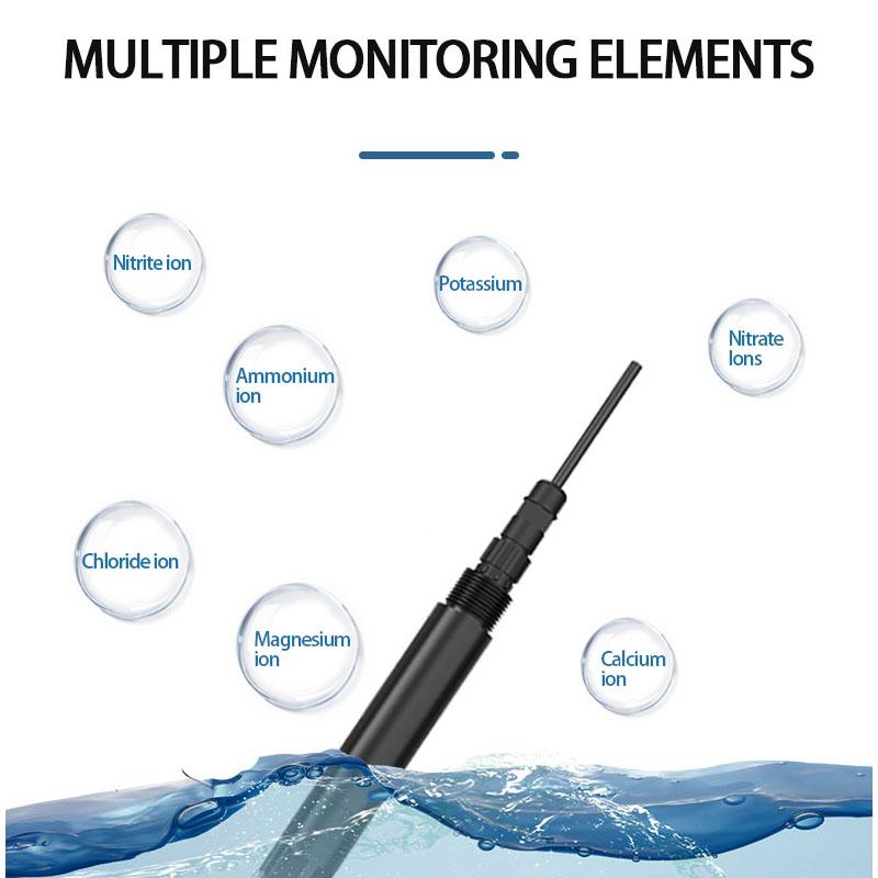
Essential Metrics:
pH, Conductivity/TDS (Total Dissolved Solids), ORP (Redox Potential), Turbidity, Temperature.
Key Contaminants: Dissolved Oxygen (DO), Chlorine (Free and Total), Ammonia, Nitrate, Phosphate.
Optional Specialty Detection: Fluoride, Chlorophyll-a (algae agent), Blue Green Algae (BGA), Hydrocarbons (Oil/Gas).
Robust Connectivity:
LoRaWAN Benefits: Our LoRaWAN water quality sensor deployments offer unmatched benefits for widespread monitoring:
Long Range: Covers vast areas with minimal infrastructure (up to 15+ km in rural areas, 2-5 km in urban areas).
Deep Penetration: Provides reliable signal through challenging environments such as dense urban areas or underground sites.
Ultra-Low Power: Battery life is measured in years, significantly reducing maintenance frequency and costs.
Scalable and Secure: Easily add thousands of sensors to a single network with enterprise-grade security.
Intelligent Data Platform: Raw sensor data turned into actionable insights:
Real-time dashboard with configurable alerts and alarms for critical parameter thresholds.
Historical trend analysis and customizable reports.
Predictive maintenance insights into sensor health.
Secure cloud-based data access from anywhere.
ZoneWu’s sensor-based water quality monitoring system provides tangible value across a variety of sectors:
1. Municipal Water and Wastewater Management:
Source Protection: Continuously monitor rivers, lakes and reservoirs for pollution events (e.g. chemical spills, algal blooms).
Treatment Optimization: Real-time adjustment of chemical dosage (coagulants, disinfectants) based on influent quality, improving efficiency and reducing costs.
Distance Network Integrity: Detect leaks (via pressure/quality anomalies) and prevent contamination from entering. Ensure residual disinfectant levels are maintained throughout the system.
Wastewater Compliance: Continuous discharge monitoring of regulatory parameters (BOD, COD, TSS, ammonia, etc.) ensures discharge permits are met and fines are avoided. Optimize aeration energy use at treatment plants.
2.Aquaculture and Fisheries:
Optimal Fish Health: Continuous monitoring of dissolved oxygen, pH, temperature and ammonia is essential to prevent fish kills and promote growth. Receive instant alerts if levels are outside safe ranges.
Feed Optimization: Reduce waste and costs by correlating feeding schedules with water quality conditions that affect fish appetite.
Disease Prevention: Maintain ideal water quality conditions to reduce stress and disease susceptibility.
3.Industrial Process & Wastewater Control:
Cooling Tower Management: Control scaling, corrosion, and biological growth (Legionella risk) by accurately monitoring pH, conductivity, ORP, and biocide levels. Optimize blowdown cycles.
Boiler Feed Water: Ensure strict quality control (pH, conductivity, dissolved oxygen) to maximize efficiency and prevent costly damage.
Environmental Compliance: Real-time monitoring of allowable parameters for industrial wastewater discharges, ensuring compliance and avoiding downtime or penalties. Early leak detection.
4. Environmental Monitoring & Research:
Watershed Health: Long-term, remote deployment of LoRaWAN water quality sensors in rivers, streams, lakes, and coastal areas to track pollution sources, nutrient loading (eutrophication), and ecosystem health trends.
Agricultural Runoff: Monitor the impact of fertilizers and pesticides on nearby water bodies.
Early Warning Systems: Rapidly detect sudden pollution events or harmful algal blooms (HABs) for rapid response.
Why choose our smart water quality sensor solutions?
Our systems are engineered for reliability, accuracy and ease of deployment:
High accuracy and stability: Industry-leading sensors with advanced calibration algorithms and drift compensation provide reliable data.
Designed for harsh environments: IP68/NEMA 6P-rated enclosures, corrosion-resistant materials and biofouling mitigation options ensure performance in the harshest conditions (wastewater, seawater, industrial environments).
Easy deployment and scalability: Modular design, simple integration (Modbus, API) and plug-and-play LoRaWAN water quality sensor connectivity enable fast setup and expansion.
Total cost of ownership Low: Minimal maintenance (long sensor life, easy cleaning/calibration), ultra-low power consumption and reduced labor costs compared to manual sampling.
Global certifications and compliance: Designed and tested to relevant international standards (e.g. CE, RoHS).
Protecting public health and safety with confidence
Learn more about our water sensor products
Contact our experts, Discuss your specific monitoring challenges and goals
Technical Consultant Email: qui@zonewu.com