As we all know, when converting electrical energy, we always rely on devices like transformers and adapters. But how are these components actually made? Let's break it down.

The transformer bobbin, also known as the coil former or frame, is the main structural component of a transformer.

Here is the full description:

act on :

Provide winding space: Provides space for the copper wire in the transformer to wind, ensuring the winding can be arranged orderly, enabling the transformer to achieve normal electromagnetic conversion function.

Fixed magnetic core: The magnetic core of the transformer is fixed in the appropriate position to ensure the integrity and stability of the magnetic circuit, and to prevent the magnetic core from displacement during the operation of the transformer.

The designed wire routing path: The wire grooves in the bobbin provide the path for the transformer to wind the wire, so that the copper wire can be wound on the bobbin accurately according to the design requirements.

Electrical connection implementation: The metal pins in the bobbin act as support pillars for the transformer's copper wire winding. After soldering, they connect to the PCB board, enabling electrical conduction during transformer operation and establishing the electrical link between the transformer and external circuits.Such as,Motorcycle drive power supply PQ20 transformer bobbin.

High power drive power off transformer bobbin

Determine the installation direction and pin sequence: The protrusions, recesses, or chamfers on the bobbin determine the transformer's placement direction or pin sequence during use, ensuring proper installation on the circuit board.

classify :

Magnetic core models include EI, EE, EF, EPC, ER, RM, PQ,PM and UU, with each type further classified by core size (e.g., EE5, EE8, EE13).

By shape: it can be divided into vertical and horizontal.For example, the EF20 LED lighting driver transformer bobbin.

DVD player switch transformer bobbin

According to the working frequency, it is divided into high-frequency bobbin and low-frequency bobbin. The high-frequency bobbin is suitable for transformers with high working frequency, while the low-frequency bobbin is suitable for transformers with low working frequency.

Pin types are classified as DIP (Direct Insert Pin) and SMD (Surface Mount Device) for their application: DIP pins are inserted into circuit board sockets, while SMD components are surface-mounted and soldered directly onto the board.Take the EE10 notebook computer power switch transformer bobbin as a reference.

Mobile phone fast charging transformer bobbin

Materials: High-strength insulating materials such as epoxy resin and polyimide are typically used. These materials not only provide excellent mechanical strength to withstand the weight of windings and electromagnetic forces, but also offer superior insulation properties to effectively prevent current leakage and short circuits.

The production process typically involves mold design and manufacturing, injection molding, and burr removal. Mold design must meet customer specifications by considering dimensions, structure, and demolding requirements. Injection molding involves injecting molten material into the mold cavity and allowing it to solidify upon cooling. Burr removal specifically targets bakelite-type bobbins to eliminate surface defects formed during the molding process.

Choosing a transformer bobbin based on specific application requirements is paramount. So, do you now have a deeper understanding of transformer bobbins? If you have any product-related questions, please feel free to contact us at any time.


Email: sales008@mycoiltech.com

Whats app ID: +86 18788862885

Name:Alex~Mycoiltech


With the rapid development of the Internet of Things, RFID and NFC technologies are becoming essential tools for smart identification, tracking, and access control. At OEM RFID Factory, we focus on providing reliable, customizable, and cost-effective RFID products for global clients across various industries.


As a professional manufacturer with years of production experience, we offer a complete range of RFID solutions, from design and material selection to mass production and quality control, helping brands bring their smart products to market faster.


Custom RFID Sticker Label for Multiple Applications

A custom RFID sticker label is one of the most widely used RFID products due to its flexibility and ease of application. These labels can be customized in size, shape, chip type, antenna design, and printing to meet different project requirements.


Our RFID sticker labels are commonly used in logistics tracking, asset management, retail inventory, library systems, and product authentication. With stable performance and strong read accuracy, they can be seamlessly integrated into existing RFID systems. OEM and ODM services are available to ensure the label matches your brand identity and technical needs.

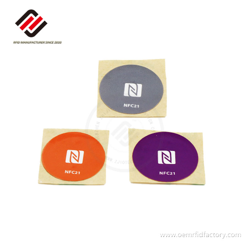
RFID sticker label

Eco-Friendly and Cost-Effective Paper NFC Sticker

For projects that require lightweight, eco-friendly, and low-cost solutions, the paper NFC sticker is an ideal choice. Made with paper-based materials, this type of NFC sticker is suitable for smart packaging, promotional campaigns, event management, and digital marketing applications.


Despite its thin and flexible structure, our paper NFC stickers maintain reliable chip performance and consistent reading distance. They can be printed with logos, QR codes, or variable data, making them a powerful tool for brand interaction and smart information sharing.


Durable RFID Key Fobs for Secure Access Control

RFID key fobs are widely used in access control systems for offices, residential buildings, hotels, gyms, and parking facilities. Designed for daily use, our key fobs are durable, waterproof, and available in multiple materials such as ABS, PVC, and epoxy.


We support customization in shape, color, chip type, and logo branding, helping clients create secure and recognizable access solutions. With strict quality inspection and stable supply capacity, our RFID key fobs are trusted by system integrators and distributors worldwide.


Why Choose RFID Factory

At www.oemrfidfactory.com, we are more than just a supplier. We are a manufacturing partner dedicated to long-term cooperation. Our advantages include:

In-house factory with strict quality control

Full OEM/ODM customization support

Stable production capacity and competitive pricing

Fast response and professional technical support

Global export experience for B2B clients


Whether you need RFID labels, NFC stickers, or access control products, we provide scalable solutions tailored to your project requirements.


Start Your RFID Project with Us

If you are looking for a reliable RFID manufacturer to support your business, OEM RFID Factory is ready to help. Explore our product range and learn more about our customization capabilities by visiting www.oemrfidfactory.com.

Feel free to contact us to discuss your RFID or NFC project and get a professional solution designed for your market.

How Does an RF-10 PCB Combine High Thermal Conductivity for Reliable RF Circuits?


In high-frequency circuit design, reliability is not merely about robust construction—it’s about maintaining precise electrical performance under varying thermal, mechanical, and environmental stresses. The RF-10 PCB with a 25mil core and Immersion Gold finish excels in this regard by integrating two cornerstone material properties: high thermal conductivity and exceptional dimensional stability. Here’s how this combination ensures long-term reliability in demanding RF applications.


1. The Role of High Thermal Conductivity (0.85 W/mk)

Mechanism:

Unlike standard FR-4 laminates,Taconic RF-10 is a ceramic-filled PTFE composite. The ceramic particles (typically aluminum oxide or similar) dispersed within the polymer matrix create efficient pathways for heat transfer. This gives the unclad laminate a thermal conductivity of 0.85 W/mk, which is significantly higher than that of conventional high-frequency substrates.


Benefits for RF Circuit Reliability:


Effective Heat Dissipation: Active components (e.g., power amplifiers, LNAs) and passive dissipative elements generate heat during operation. TheRF-10 substrate acts as a lateral heat spreader, drawing heat away from localized hotspots. This prevents excessive temperature rise that could:


Shift component operating points.

Degrade solder joint integrity.

Accelerate aging of the material itself.


Reduced Thermal Gradient: A more uniform board temperature minimizes the risk of thermally-induced stress fractures in solder joints and plated through-holes (vias), which are critical for the 44 vias and 41 through-hole pads in a typical design using this board.


Enhanced Power Handling: For circuits handling moderate power levels (e.g., in power dividers or antenna feed networks), better heat dissipation allows for safer, more reliable operation without derating.


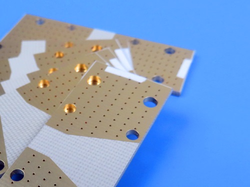
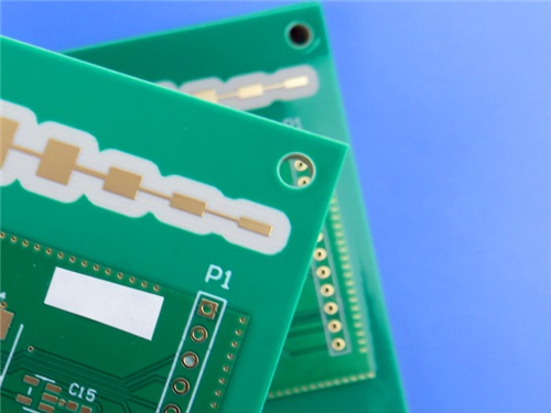
RF-10 PCB 2-layer 25mil


2. The Critical Importance of Dimensional Stability (Low CTE & Moisture Resistance)

Mechanism:

Dimensional stability in RF-10 Taconic RF PCB Circuit Board is achieved through two key factors:


Ceramic Filler: The inorganic ceramic filler has a inherently low coefficient of thermal expansion (CTE).


Woven Fiberglass Reinforcement: The thin glass fabric provides a rigid, stable scaffold that constrains the polymer's natural tendency to expand.


This results in remarkably low CTE values:


x-CTE: 16 ppm/°C

y-CTE: 20 ppm/°C

z-CTE: 25 ppm/°C


Furthermore, the PTFE-based matrix has very low moisture absorption (0.08%), preventing swelling and property changes in humid environments.


Benefits for RF Circuit Reliability:


Stable Impedance and Resonance: The core function of an RF circuit (e.g., a filter or antenna) depends on precise physical dimensions. A trace's width and its distance to the ground plane define its characteristic impedance. With low in-plane (x, y) CTE, the geometry of critical transmission lines (like microstrips on this 2-layer board) remains constant across temperature fluctuations, ensuring minimal drift in impedance and resonant frequency.


Via and Plated Hole Integrity: The matched CTE between the RF-10 core and the copper plating (via plating thickness: 20μm) reduces cyclical stress on the barrel of the vias during thermal cycling. This dramatically lowers the risk of interconnect failure—a common reliability issue in less stable substrates.


Improved Assembly and Operational Yield: A board that doesn't warp or expand excessively during the solder reflow process (which involves high temperatures) ensures better solder paste deposition and component alignment. This leads to fewer defects and stronger mechanical bonds.


3. Synergistic Effect: How They Work Together for Ultimate Reliability

The true reliability advantage emerges from the synergy between thermal conductivity and dimensional stability:


Preventing Thermal Runaway Scenarios: High thermal conductivity quickly removes heat, limiting the board's overall temperature rise. Because dimensional change (expansion) is directly proportional to temperature change (ΔT), a lower operatingΔT directly results in less physical expansion. The low CTE then ensures that the minimal expansion that does occur is itself highly constrained.


Maintaining Performance in Real-World Environments: Consider an aircraft collision avoidance system or an outdoor GPS antenna. The board must operate from cold high-altitude skies to sun-baked enclosures. The RF-10 Taconic PCB manages this by:


Efficiently dissipating internal heat from components.


Resisting expansion/contraction from external ambient changes.


This dual action keeps the electrical phase length, impedance, and grounding consistent, so the circuit performs identically at -40°C as it does at +85°C.


Long-Term Durability: The reduction in cyclical thermal stress on copper traces, vias, and component joints minimizes fatigue-related failure mechanisms. This leads to a longer mean time between failures (MTBF), which is paramount for aerospace, defense, and satellite applications where repair is impossible.


Conclusion: A Foundation Built for Rigorous Demands

The RF-10 2-layer PCB is more than just a platform for components; it is a stable, thermally-competent foundation engineered for the rigors of RF service. By combining high thermal conductivity (0.85 W/mk) for proactive heat management with exceptional dimensional stability (low CTE & moisture absorption) for geometric and electrical consistency, it directly addresses the primary physical threats to RF circuit reliability. This allows designers to focus on pushing performance boundaries, confident that their underlying substrate will not be the source of field failures, signal drift, or unexpected performance degradation. For missions where failure is not an option, this material synergy is not just a benefit—it is a requirement.


How Does the 30mil Dk 3.3 RO4533 Optimize Performance in RF PCB Designs?


In the precise engineering realm of radio frequency (RF) and microwave circuit design, every material parameter serves a specific function. Rogers RO4533 laminate achieves an optimal balance for many antenna and RF applications through two defining characteristics: a 30mil (0.762mm) Rogers substrate thickness and a stable Dielectric Constant (Dk) of 3.3. Together, these parameters form the foundation for predictable, high-performance, and manufacturable circuit boards. This article explains how each factor independently and synergistically optimizes RF PCB performance.


The Foundation: Stable Dk 3.3 for Predictable Electrical Behavior

The Dielectric Constant (Dk orεᵣ) is a measure of how much a material concentrates electric flux. In RF design, the value is important, but its stability over frequency, temperature, and lot-to-lot manufacturing is paramount.


1. Precision Impedance Control and Signal Integrity

Transmission lines (microstrip, stripline) require precise characteristic impedance (typically 50Ωor 75Ω). The impedance calculation depends directly on the Dk of the substrate. RO4533's consistent Dk of 3.3 at 10 GHz allows engineers to:


Design with Confidence: Simulation models using this Dk value accurately predict real-world performance, reducing design iterations.


Achieve Manufacturing Consistency: PCBs from different production runs maintain identical electrical characteristics, ensuring every unit performs as specified.


Maintain Signal Integrity: A stable Dk prevents impedance mismatches that cause signal reflections, minimizing insertion loss and maximizing power transfer.


2. Optimized Antenna Resonance and Size

For patch antennas—a key application for RO4533—the resonant length of the radiating element is inversely proportional to the square root of the Dk. A Dk of 3.3 offers a strategic balance:


It allows for a physically smaller antenna compared to using a lower-Dk material (e.g., Dk 2.2), saving valuable board space.


It avoids the excessive electrical "shrinkage" and manufacturing sensitivity associated with very high-Dk materials, preserving bandwidth and radiation efficiency.


3. Stable Phase Response for Complex Systems

In phased-array antennas and sensitive filters, the electrical length and phase response are critical. Rogers 4533's low loss (Df 0.0025) and stable Dk ensure that the phase velocity of signals is predictable and consistent, enabling accurate beamforming and stable filter cutoffs across the operating band.


RO4533 PCB 30mil


The Structural Lever: 30mil Thickness for Performance Tuning

Substrate thickness is a powerful degree of freedom for the RF designer, directly influencing bandwidth, efficiency, isolation, and thermal performance.


1. Enhanced Bandwidth for Antenna Applications

For patch antennas, bandwidth is directly proportional to substrate thickness. A 30mil (0.76mm) substrate provides significantly wider operational bandwidth than a thinner alternative (e.g., 20mil). This is crucial for modern wireless standards (4G/LTE, 5G) that require antennas to cover broad frequency ranges. The 30mil thickness offers an optimal trade-off, delivering substantial bandwidth without the mechanical bulk and potential higher-order mode excitation of excessively thick substrates.


2. Practical Impedance Realization

For a standard 50-ohm microstrip line on a Dk 3.3 material, a 30mil thickness results in a trace width that is ideal for manufacturing and performance.


The calculated width (~65-70 mils for 1oz copper) is neither excessively narrow (which increases loss and etching difficulty) nor overly wide (which consumes space).


This practical geometry supports fine-feature capabilities (down to 4/5 mil trace/space) for complex RF circuitry while maintaining robust, low-loss transmission lines.


3. Improved Circuit Isolation and Reduced Parasitics

A thicker dielectric increases separation between the signal layer and ground plane, which:


Reduces parasitic capacitance between traces and the ground plane.


Improves isolation between adjacent circuit elements, minimizing unwanted coupling and crosstalk.


For two-layer designs, it establishes a more well-defined ground reference, improving antenna pattern predictability and front-end circuit stability.


4. Mechanical and Thermal Robustness

The 0.762mm core provides a sturdy mechanical base, improving board rigidity and handling reliability. Combined with RO4533's relatively good thermal conductivity (0.6 W/m/K), this thickness aids in spreading heat from active components like power amplifiers, contributing to better thermal management and long-term reliability.


The Powerful Synergy: 30mil and Dk 3.3 Working in Concert

The true optimization emerges from the interaction of these two properties.


Predictable Effective Dk: In a microstrip line, the signal experiences an "effective Dk" between 1 (air) and the Dk 3.3 Rogers substrate. The 30mil thickness, relative to the practical trace width, results in an effective Dk that ensures strong field confinement within the substrate. This maximizes efficiency, minimizes radiative losses, and makes performance highly predictable through simulation.


Inherent Design for Manufacturing (DfM): This combination naturally leads to geometries compatible with high-yield PCB fabrication. It avoids the extreme aspect ratio drilling challenges of very thick boards and the delicate trace structures of very thin boards, supporting reliable plating (like 20μm via plating) and robust assembly.


Stable Performance Under Stress: RO4533’s high Tg (>280°C) and matched CTE to copper ensure that the critical 30mil thickness and the Dk value remain stable across temperature fluctuations during soldering and operation. This preserves the carefully designed electrical relationships in the field.


Conclusion: An Engineered Solution for High-Frequency Success

The specification of 30mil RO4533 PCB with a Dk of 3.3 represents a deeply optimized solution for a wide range of RF applications. It is not a default but a conscious choice that delivers:


Electrical Predictability through material stability.

Enhanced Performance through optimized bandwidth and low-loss characteristics.

Manufacturing Resilience through practical geometries and robust material properties.


For designers of cellular infrastructure, point-to-point radios, and aerospace communication systems, this material configuration provides a reliable, high-performance canvas. It simplifies the design process by reducing performance uncertainty and enables the creation of circuits and antennas that perform reliably from prototype through high-volume production. When your design priorities include signal integrity, bandwidth, and real-world reliability, the 30mil RO4533 laminate stands as a proven, performance-optimized foundation.

What Are the Key Advantages of Using F4BM220 Laminate for High-Frequency 2-Layer PCBs?


For engineers designing high-frequency circuits, selecting the right PCB substrate is a critical decision that directly impacts performance, reliability, and cost. When it comes to 2-layer boards for RF, microwave, and fast digital applications, F4BM220 laminate emerges as a superior choice over standard FR-4 and even other PTFE-based materials. Its advantages are rooted in a unique formulation that balances electrical performance, mechanical stability, and manufacturability.


Here are the key advantages of using F4BM220 substrate for yourhigh-frequency 2-layer PCBs:


1. Exceptionally Low Signal Loss at High Frequencies

The primary advantage of Wangling F4BM220 is its outstanding electrical performance in the GHz range.


Ultra-Low Dissipation Factor (Df): At 10 GHz, its Df is a mere 0.001. This is an order of magnitude lower than standard FR-4, resulting in significantly reduced dielectric signal loss. For 2-layer PCBs, where trace lengths are direct and signal integrity is paramount, this minimizes attenuation, preserves signal strength, and improves the overall efficiency of power amplifiers, filters, and transmission lines.


Stable, Low Dielectric Constant (Dk): With a Dk of 2.2±0.04 at 10 GHz, F4B DK2.2 allows for precise and predictable impedance control (e.g., 50Ωtransmission lines). Its remarkably low thermal coefficient of Dk (-142 ppm/°C) ensures this impedance remains stable across a wide operational temperature range (-55°C to 150°C), preventing performance drift in varying environments.


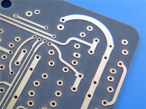
F4BM220 PCB


2. Enhanced Mechanical and Dimensional Stability

High-frequency circuits are often sensitive to physical deformation, which can alter electrical lengths and performance.


Matched, Low CTE: F4BM220 offers a low and well-matched Coefficient of Thermal Expansion in the X and Y axes (25 and 34 ppm/°C). This closely matches the CTE of copper, reducing stress on plated through-holes (vias) and solder joints during thermal cycling. For a 2-layer board, this translates to exceptional long-term reliability, especially in applications subject to temperature fluctuations like outdoor antennas or automotive radar.


Minimal Moisture Absorption: With water absorption of≤0.08%, F4BM220 is highly resistant to humidity. This prevents the common issue of Dk and Df values shifting in humid environments, ensuring consistent performance from factory to field deployment.


3. Optimal Balance for Thin-Core, High-Performance Builds

The 0.5mm core thickness specification is particularly well-suited to F4BM220.


Stiffness in Thin Profiles: The material's composition provides excellent rigidity even in thin cores, preventing board flex that could damage components or affect performance. This makes it ideal for compact, lightweight modules common in modern aerospace, portable communications, and phased array systems.


Controlled Impedance in Simple Stackups: For 2-layer designs, achieving precise controlled impedance can be challenging. The stable Dk of F4BM220, combined with a well-defined thin core, allows designers to calculate and achieve target impedance (e.g., microstrip lines) with high confidence and reproducibility.


4. Superior Thermal Performance and Reliability

High Decomposition Temperature: The PTFE-based material can withstand temperatures up to 288°C, ensuring it remains stable during assembly processes like soldering and rework.


V0 Flammability Rating: It meets the UL-94 V0 standard, a critical requirement for many commercial and aerospace applications, enhancing the safety and compliance of the final product.


5. Cost-Effective Performance for Non-Critical PIM Applications

Within the family of high-performance PTFE laminates, F4BM220 offers a strategic advantage:


It uses Electrodeposited (ED) copper foil, which is more cost-effective than specialized foils. While its companion material F4BME220 (with RTF foil) is necessary for ultra-low Passive Intermodulation (PIM) applications like sensitive receiver front-ends, F4BM220 is the optimal, cost-efficient choice for the vast majority of high-frequency applications where PIM is not the primary concern, such as power amplifiers, filters, and many antenna elements.


Conclusion: The Ideal Foundation for Demanding 2-Layer Designs

In summary, choosing F4BM220 high frequency laminate for a 2-layer PCB provides a compelling trifecta of low electrical loss, outstanding mechanical stability, and practical manufacturability. It elevates the performance ceiling of double-sided boards, enabling them to function reliably in demanding high-frequency scenarios where FR-4 would fail. By ensuring signal integrity, impedance stability, and rugged reliability in a thin-profile format, F4BM220 DK2.2 F4B PTFE PCB allows engineers to push the boundaries of RF and microwave design without moving to more complex and costly multilayer architectures. For applications ranging from satellite communications and radar to base station antennas and test equipment, it represents a foundational material choice that guarantees performance from the substrate up.


Why Choose a Hybrid PCB Construction? 

Benefits of Combining RO4350B and FR-4 in a 4-Layer Hybrid PCB.


In the world of advanced electronics, especially for RF, microwave, and high-speed digital applications, the choice of Printed Circuit Board (PCB) materials is a critical decision that directly impacts performance, reliability, and cost. A purely high-performance laminate like Rogers RO4350B offers superior electrical characteristics but at a premium.Standard FR-4 is cost-effective and robust but lacks the necessary performance for critical high-frequency circuits. This is where the intelligent hybrid construction—specifically combining a RO4350B core with FR-4 in a 4-layer PCB stack-up—emerges as the optimal engineering compromise. Here’s a detailed breakdown of the key benefits.


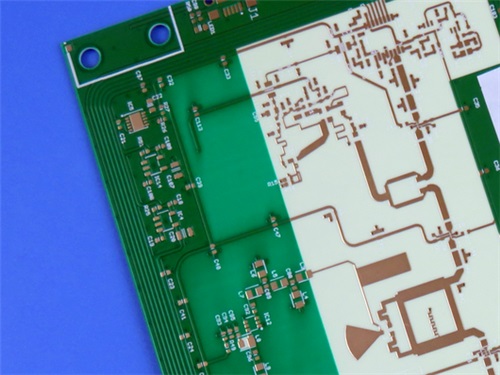
4-layer Hybrid PCB RO4350B+FR4


1. Optimal Cost-Performance Ratio (The Core Benefit)

This is the primary driver for choosing a hybrid design.


Targeted Performance: Instead of constructing the entire board from expensive high-frequency laminate, you use Rogers 4350B only where it matters most—for the critical signal layers carrying RF or high-speed signals. In our featured 4-layer stack-up, the outer layers (L1 & L4) are built on the 0.508mm RO4350B core, ensuring minimal signal loss and stable impedance for your most sensitive traces.


Cost Containment: The inner layers (L2 & L3), typically used as solid ground and power planes, are fabricated using reliable, industry-standard TG170 FR-4. FR-4 is significantly less expensive than specialized RF laminates and is perfectly suited for this purpose, providing excellent electrical isolation and structural rigidity without compromising the board's function. This strategic partitioning can reduce overall material costs by 20-40% compared to an all-RO4350B board.


2. Superior Electrical Performance Where It Counts

The hybrid PCB design directly leverages the standout electrical properties of RO4350B for signal integrity:


Low and Stable Dielectric Constant (Dk=3.48±0.05): This ensures predictable impedance control (e.g., 50-ohm transmission lines) on your RF paths, reducing signal reflection and mismatch.


Extremely Low Dissipation Factor (Df=0.0037): This minimizes dielectric loss at high frequencies (e.g., 10 GHz and beyond), preserving signal strength and integrity for applications like cellular antennas, automotive radar, and satellite LNBs. The FR-4 inner layers, not carrying high-speed signals, do not detrimentally affect this performance.


3. Enhanced Thermal Management and Mechanical Stability

The combination of materials addresses both thermal expansion and reliability concerns.


Matched CTE to Copper: RO4350B has a Coefficient of Thermal Expansion (CTE) closely matched to copper. This excellent dimensional stability is crucial in a hybrid structure, preventing stress, delamination, and via failure at the material interface during thermal cycles.


High Tg (>280°C) and Low Z-Axis CTE: RO4350B's high glass transition temperature and low expansion through the board's thickness ensure that plated through-holes (PTHs—your 125 vias) remain reliable even under severe thermal shock, a common requirement in automotive and outdoor infrastructure applications.


4. Simplified Manufacturing and FR-4 Process Compatibility

Unlike pure PTFE-based microwave materials, RO4350B is designed for ease of fabrication.


Seamless Integration: RO4350B processes like FR-4. It uses standard drilling, desmear, and plating techniques. This means your hybrid board can be manufactured on standard PCB production lines without the need for special processes, exotic chemistries, or costly handling procedures required for PTFE.


Predictable Yield and Lead Time: This common processability streamlines production, leading to higher manufacturing yields, faster turnaround times, and reduced fabrication risk and cost. It simplifies the lamination process when bonding the RO4350B core to the FR-4 prepreg and core.


5. Structural Rigidity and Design Versatility

The hybrid circuit board stack-up creates a robust, versatile platform.


FR-4 Provides Robust Backbone: FR-4 offers excellent mechanical strength, making the final 0.98mm thick board durable and resistant to warpage. This is important for larger boards or those used in high-vibration environments.


Ideal for Multi-Function Designs: This construction is perfect for modern modules that combine RF front-ends with digital control and power sections. You can route sensitive RF lines on the RO4350B-based outer layers while using the inner FR-4 layers for power distribution, digital grounding, and lower-speed signaling—all in one compact, reliable package.


Conclusion: Who Should Choose This Hybrid Construction?

The 4-layer hybrid PCB with RO4350B and FR-4 is not a one-size-fits-all solution, but it is the engineer's smart choice for specific, high-value applications:


When your design has defined critical signal paths (e.g., antenna feeds, filter networks, RF transceivers) alongside supporting digital logic.


When system cost is a constraint, but performance on key circuits cannot be compromised.


When reliability under thermal stress is required (e.g., automotive, telecom outdoors).


When you need the electrical performance of a high-end laminate but with the supply chain simplicity and proven manufacturability of FR-4.


In essence, choosing this hybrid RO4350B FR4 4-layer PCB construction is a strategic decision to allocate your budget precisely where it delivers the highest return: unparalleled electrical performance for critical circuits, without over-engineering and over-spending on the entire board. It represents the optimal balance between the cutting-edge capabilities of advanced materials and the pragmatic economics of volume electronics manufacturing.


Underwater connectors are critical components in deep-sea engineering, where reliability directly determines the safety and success of marine operations. To ensure stable performance under extreme conditions, WAIN employs a comprehensive and systematic testing program.

Mechanical performance tests—including hydrostatic pressure tests, pressure cycling, and vibration testing—simulate real deep-ocean environments.

Durability tests, such as aging and temperature-rise evaluations, assess long-term stability.

Electrochemical and insulation tests ensure electrical safety under prolonged exposure to seawater.

Environmental adaptation tests—including seawater immersion, volume-change resistance, and compression deformation—validate corrosion resistance and structural integrity.

Through multi-dimensional verification, WAIN guarantees that its underwater connectors operate reliably in complex marine environments.

WAIN waterproof and subsea connectors are now widely used in deep-sea resource exploration, marine engineering equipment, underwater ROVs, subsea seismic systems, diving systems, underwater imaging devices, and deep-ocean lighting applications.


Merry Christmas!

As sparkling lights bring communities together, we hope your season is filled with warmth, joy, and meaningful moments with those you cherish.
We extend our heartfelt thanks for your trust and partnership throughout the past year. It is a privilege to collaborate with you, and we look forward to continuing our journey together in the year ahead.
From all of us at WAIN, we wish you a holiday season brimming with joy, peace, and warmth. May the coming year bring you renewed inspiration and continued success.

In industrial automation and precision equipment, trapezoidal lead screws are the core transmission mechanism for achieving rotary-to-linear motion, directly affecting the accuracy and stability of the equipment. However, practitioners often suffer from decreased equipment efficiency and shortened lifespan due to a lack of in-depth understanding of the principles and improper selection. This article will break down the motion principle of trapezoidal lead screws and provide a practical selection guide.

I. Product Motion Principle and Related Parameters

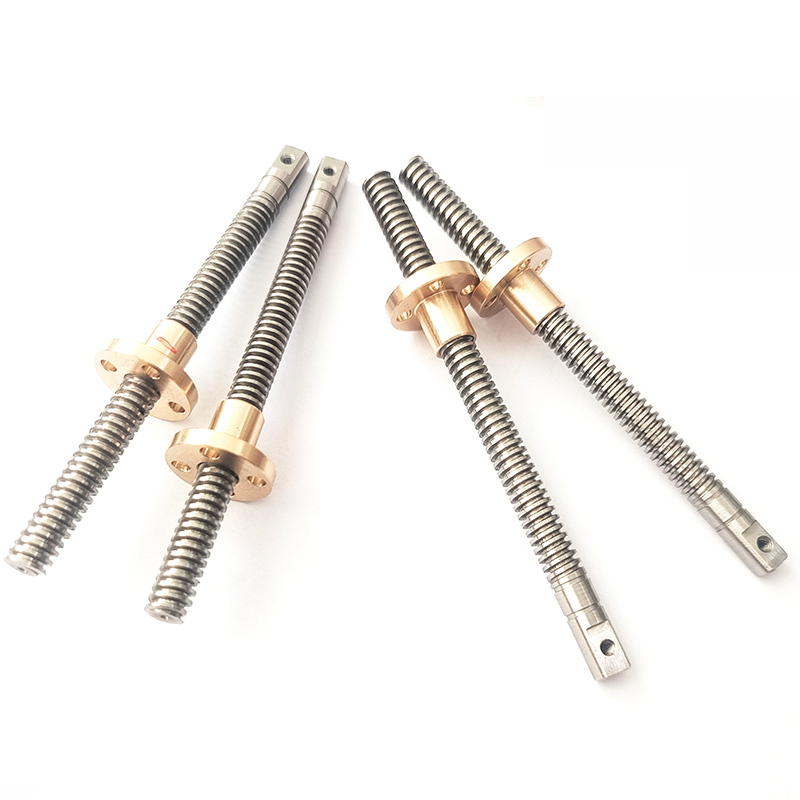
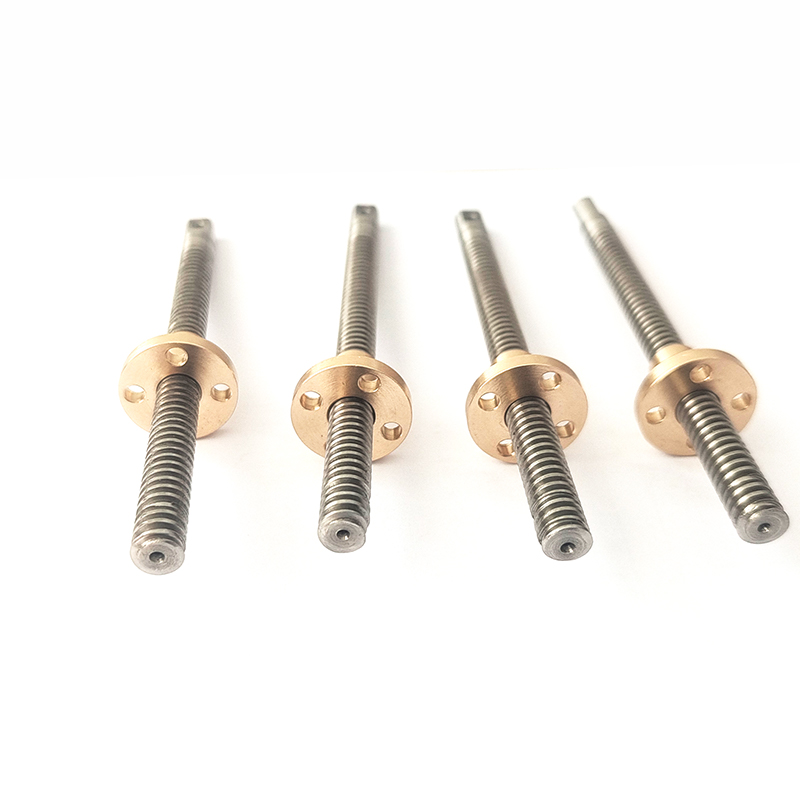
1. Motion Principle: The trapezoidal lead screw converts rotational motion into linear motion through the meshing of the screw and nut, simultaneously transmitting energy and power.


II. Product Features

1. Simple structure, convenient processing and operation, and economical cost;

2. Self-locking function is achieved when the thread helix angle is less than the friction angle;

3. Smooth and stable transmission process;

4. Relatively high frictional resistance, with a transmission efficiency in the range of 0.3~0.7. In self-locking mode, the efficiency is below 0.4;

5. Possesses a certain degree of impact and vibration resistance;

6. Overall load capacity is stronger than that of ordinary rolling screws.


III. Selection and Verification Calculations

For general force-transmitting screws, the main failure modes are thread surface wear, fracture under tensile stress, shearing, and shearing or bending at the thread root. Therefore, the main dimensions of the screw drive are determined primarily based on wear resistance and strength calculations during design.

For transmission screws, the main failure mode is excessive clearance due to wear or deformation leading to decreased motion accuracy. Therefore, the main dimensions of the screw drive should be determined based on thread wear resistance and screw stiffness calculations during design. If the transmission screw also bears a large axial load, its strength needs to be additionally calculated.

Long screws (slenderness ratio exceeding 40) that are not manually adjustable may produce lateral vibration; therefore, their critical speed needs to be checked.

IV. Usage Precautions

1. Load Considerations: Additional radial loads should be avoided as much as possible, as such loads can easily cause screw malfunction, increased wear, and jamming.

2. Dust Prevention Requirements: Foreign objects must be prevented from entering the thread. If impurities such as iron filings, tin dross, and aluminum shavings are easily generated under operating conditions, a protective cover should be installed to prevent foreign objects from entering the thread and causing abnormal wear or jamming.

3. Slenderness ratio requirement: When the slenderness ratio exceeds a certain range (60 or above), the screw will bend due to its own weight, resulting in radial off-center load on the nut. Depending on the actual operating speed and torque, this may lead to abnormal wear, jamming, shaft end bending, or even breakage. To solve this problem, an anti-runout device can be installed in the middle of the screw for constraint.

4. During installation, attention should be paid to the coaxiality and levelness calibration of the fixed-support installation method; for the fixed-free cantilever structure, attention should be paid to the control of shaft end tolerances and the locking and reinforcement of the head.

5. When installing a trapezoidal thread screw, runout verification must be performed. If suitable measuring equipment is lacking, the screw can be moved by hand along its entire length once or multiple times before installing the driving component. If the force required to move the outer diameter of the shaft is uneven and accompanied by wear marks, it indicates that the lead screw, nut support, and guide rail are not aligned. In this case, first loosen the relevant mounting screws, and then move the lead screw by hand once. If the required force becomes uniform at this time, the corresponding components can be recalibrated. If the force is still uneven, the mounting screws need to be loosened again to determine the location of the calibration error.

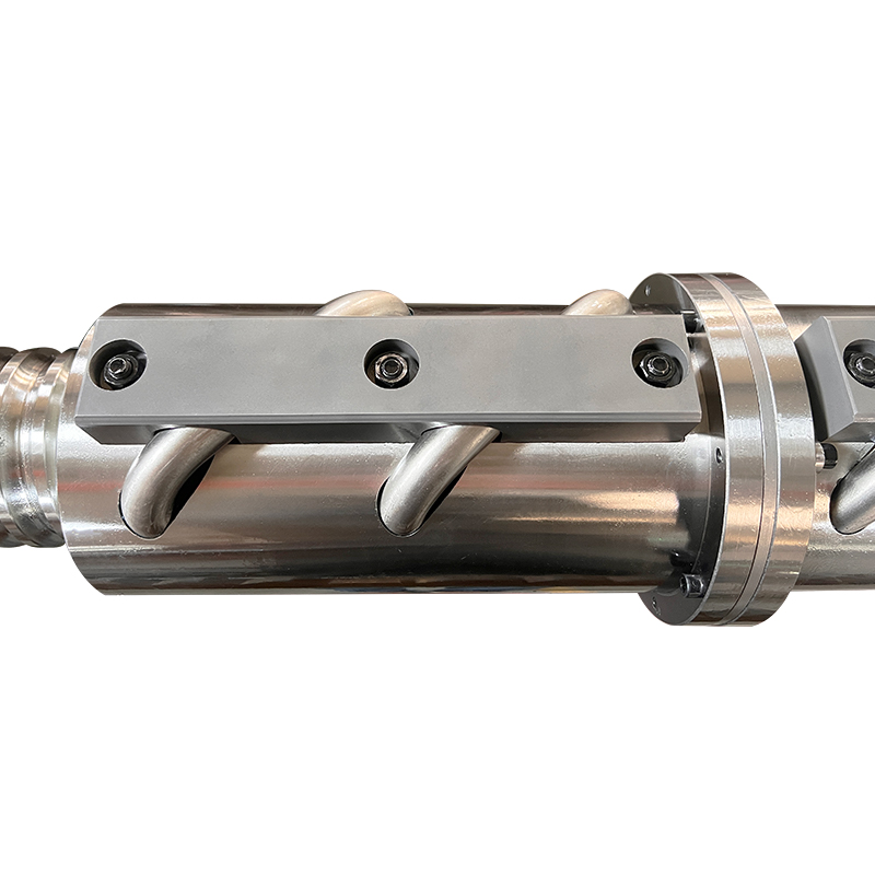
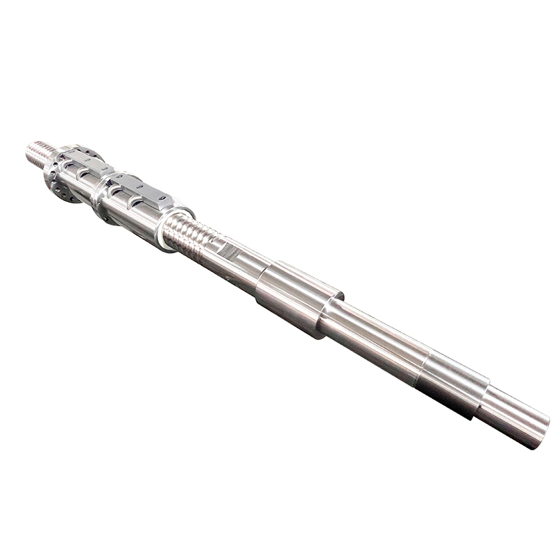
The ball screw (often called a "lead screw") of an injection molding machine is its core component, often referred to as the "heart" of the machine. Its operation is a complex process integrating physics, mechanics, and thermodynamics.

Simply put, its core task is to transport, melt, compress, and homogenize solid plastic granules, ultimately injecting the molten plastic into the mold cavity with sufficient pressure and speed.

To better understand its operation, we can divide its working cycle into the following stages: A complete working cycle of an injection molding machine ball screw. In a complete injection cycle, the ball screw mainly performs two actions: rotation and axial movement. Its working cycle can be divided into three stages:

1. Rotation (Plasticizing/Metering) Stage

Objective: To transport, heat, melt, and homogenize the solid plastic granules in the hopper.

Action: The lead screw rotates at high speed inside the barrel but does not move forward (at this time, the injection cylinder at the rear of the lead screw releases pressure, allowing the lead screw to retract due to the reaction force of the plastic during rotation).

Operation Process:

Feeding and Conveying: Plastic granules fall from the hopper into the barrel. The rotation of the screw, like a screw turning in a nut, uses the inclined plane of the thread to continuously push the plastic granules forward.

Compression and Melting: The screw structure is divided into three sections from back to front: the feeding section, the compression section, and the metering section.

Feeding Section: The thread depth is relatively deep, mainly used for stable conveying of solid granules.

Compression Section: The thread depth gradually decreases. Here, the plastic is strongly compressed and sheared, while the heating coil outside the barrel also heats it. Under the combined action of "shear heat" and "external heating," the solid plastic rapidly melts into a viscous flow state. In fact, more than 80% of the melting heat comes from the shear heat generated by the screw rotation.

Metering Section: The thread depth is the shallowest. Its main function is to further homogenize the temperature and composition of the melt, ensuring the uniform quality of the melt stored at the front end.

Result: Uniformly molten plastic is pushed to the front of the screw (at the nozzle), and the accumulated pressure (back pressure) pushes the entire screw backward, reserving a fixed amount of molten material for the next injection.

2. Axial Movement (Injection/Holding Pressure) Stage

Objective: To inject the molten plastic reserved in the previous stage into the mold cavity at high speed and high pressure.

Action: The screw stops rotating and, under the powerful thrust of the injection cylinder, moves forward at high speed as a piston.

Operation Process:

Injection: The screw advances forward at extremely high speed, injecting the molten plastic reserved in the front through the nozzle, mold runner, and gate into the closed mold cavity. This process needs to be completed in a very short time to ensure that the molten material fills every corner of the cavity simultaneously.

Holding Pressure: When the cavity is about to be filled, the injection speed slows down, transitioning to a high-pressure "holding pressure" stage. The screw continues to move forward slowly, using extremely high pressure to replenish the volume vacated by the cooling and shrinkage of the plastic, preventing defects such as shrinkage marks and insufficient material in the product.

3. Reset (Preparing for the Next Cycle)

Objective: To prepare the melt for the next injection molding cycle.

Action: After the holding pressure is completed, the screw stops axial movement and begins to rotate again (returning to the first stage) for the next plasticizing and metering. At this time, the mold opens, ejects the product, and then closes, awaiting the next injection.

Key Design Features of the Ball Screw

To accomplish the above complex tasks, the ball screw itself is designed with great precision:

Length-to-Diameter Ratio (L/D): The ratio of the ball screw's length to its diameter. A larger L/D ratio results in better plasticizing and more uniform temperature. Common ratios are between 18:1 and 25:1.

Compression Ratio: The ratio of the volume of the first threaded groove in the feeding section to the volume of the last threaded groove in the metering section. It determines the degree of plastic compression and is crucial to melting efficiency. Different plastics require different compression ratios.

Three-Stage Design: As mentioned above, the feeding section, compression section, and metering section each perform their respective functions, forming the basis for the efficient operation of the lead screw.

In summary, you can visualize the operation of an injection molding machine screw as follows:

It's like a "meat grinder": as it rotates, it bites, shears, mixes, and conveys materials.

It's like a "piston" or "syringe": as it propels forward, it injects the processed "fluid" under high pressure.

It's also a "heat generator": through its own rotational shearing, it generates most of the heat needed to melt the plastic.

This ingenious combination of "rotational plasticizing" and "axial injection" allows the injection molding machine screw to efficiently and precisely complete the transformation process from solid granules to precision plastic products.