Is TFA294 PCB the Optimal Solution for Your High-Frequency RF Design Projects?


Quick Answer

For high-frequency RF designs operating up to 40 GHz that demand stable dielectric performance across extreme temperatures and aerospace-grade reliability, TFA294 PCB is an excellent solution. Its PTFE-ceramic composite construction delivers a consistent Dk of 2.94, ultra-low dissipation factor, and near-copper CTE values, making it particularly well-suited for phased array antennas, airborne radar systems, and satellite communications equipment where frequency stability and long-term reliability are non-negotiable.


Key Takeaways


  • Wangling TFA294 uses a glass-fiber-free PTFE-ceramic composite formulation that eliminates the fiberglass effect and delivers uniform electromagnetic wave propagation across X, Y, and Z axes.


  • The material maintains a dielectric constant of 2.94 at 10 GHz with a TCDK of only -5 ppm/°C from -55°C to 150°C, ensuring exceptional phase stability in temperature-cycling environments.


  • With CTE values of 18 ppm/°C in-plane and 32 ppm/°C through-plane, TFA294 closely matches copper foil expansion, reducing thermal stress on plated through-holes and solder joints.


  • TFA294 is part of a broader TFA series with Dk options of 2.94, 3.0, 6.15, and 10.2, enabling designers to select the exact dielectric constant for impedance matching and antenna performance requirements.


  • The material achieves UL 94-V0 flammability rating and 0.03% moisture absorption, supporting deployment in aerospace, defense, and outdoor industrial environments.


1.Understanding the Demands of Modern High-Frequency PCB Design


  • As RF and microwave systems push toward higher frequencies—from sub-6 GHz 5G infrastructure to 24 GHz automotive radar, 40 GHz satellite links, and phased array defense systems—the choice of PCB substrate material moves from a secondary consideration to a defining factor of overall system performance. Engineers designing at these frequencies quickly discover that standard FR-4 materials, with their Dk of 4.4–4.6 and Df around 0.02, introduce unacceptable signal loss, impedance drift, and phase distortion.


  • This is where specialized PTFE-based high-frequency substrates enter the picture. Polytetrafluoroethylene (PTFE) resin inherently exhibits low dielectric loss and stable electrical properties, but pure PTFE suffers from poor dimensional stability and high thermal expansion. The industry solution has been to compound PTFE with ceramic fillers, creating composite materials that retain PTFE's electrical advantages while gaining mechanical rigidity and thermal management capabilities.


  • TFA294 represents one such advanced ceramic-filled PTFE substrate, engineered specifically for applications where frequency stability and environmental ruggedness are prioritized.


2.TFA294 Material Architecture and Manufacturing Approach


What distinguishes TFA294 from many competing high-frequency laminates is its manufacturing methodology. Unlike traditional PCB substrates that impregnate glass fiber cloth with resin to form prepreg sheets, the Wangling TFA series employs a fiber-free production process. Nano-scale ceramic particles are uniformly dispersed throughout the PTFE resin matrix using a proprietary mixing and forming process, creating a homogeneous dielectric core without woven reinforcement.


This glass-fiber-free construction has several profound implications for electrical performance:


  • Elimination of the fiberglass effect: In woven-reinforced substrates, the alternating resin-rich and fiber-rich regions create local Dk variations that cause signal velocity differences and phase anomalies, particularly noticeable at millimeter-wave frequencies. TFA294's uniform ceramic-PTFE matrix removes this variability.


  • Isotropic electrical behavior: With no directional fiber orientation, dielectric properties remain consistent regardless of trace routing direction on the board. This is especially valuable for phased array antennas where element-to-element phase consistency directly impacts beamforming accuracy.


  • Predictable impedance control: The homogeneous material structure enables tighter impedance tolerances, which is critical for 50-ohm transmission lines and matching networks in high-frequency amplifier designs.


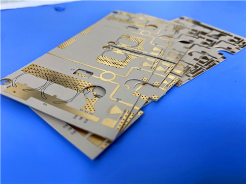
The 2-layer TFA294 PCB stackup commonly specified for antenna and microwave circuits consists of 35μm copper foil on both sides, with a 1.016 mm 40 mil TFA294 core dielectric. This configuration provides a robust mechanical platform while supporting controlled-impedance transmission lines in the 50–75 ohm range typical for RF systems.
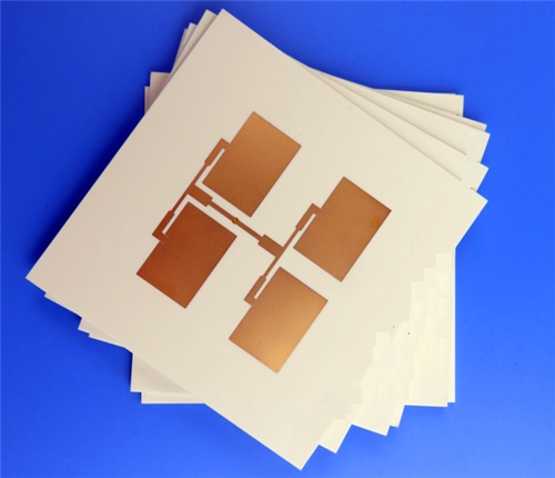
 

40mil TFA294 PCB


3.Core Electrical Performance: Data and Engineering Significance


The electrical specifications of TFA294 are not just numbers on a datasheet—each parameter directly translates to measurable system-level performance.


3.1 Dielectric Constant (Dk) and Frequency Stability


  • At 10 GHz, TFA294 exhibits a dielectric constant of 2.94. This mid-range Dk value strikes a practical balance: lower than FR-4 (which reduces signal propagation delay and enables faster edge rates) but higher than ultra-low-Dk materials like RT/duroid 5880 (Dk 2.2), allowing for more compact circuit layouts and smaller antenna element dimensions.


  • What truly sets this material apart is its dielectric stability across frequency. The dissipation factor remains 0.0010 at both 10 GHz and 20 GHz, and only increases modestly to 0.0012 at 40 GHz. For perspective, standard FR-4 typically shows Df values of 0.02 or higher at 1 GHz, meaning TFA294 delivers roughly 17×lower signal loss at microwave frequencies. For a 10 cm microstrip transmission line at 20 GHz, this difference translates to several decibels of saved signal power—power that directly contributes to increased antenna gain or extended communication range.


3.2 Temperature Coefficient of Dielectric Constant (TCDK)


  • TFA294 achieves a TCDK of -5 ppm/°C across the -55°C to 150°C operating range. This is a critical specification for systems exposed to extreme temperature swings, such as airborne electronics, outdoor base stations, and satellite payloads.


  • To put this value in context: a -5 ppm/°C TCDK means that over a 200°C temperature excursion, the dielectric constant shifts by only 0.00294—less than 0.1% deviation. For a phase-sensitive radar or phased array system, this level of stability ensures that beam steering angles remain accurate regardless of whether the equipment is operating in arctic conditions or desert heat. Systems using materials with higher TCDK values often require temperature compensation algorithms or calibration routines that add complexity, cost, and signal processing latency.


3.3 Thermal and Mechanical Reliability Characteristics


  • High-frequency circuits, particularly power amplifiers and active antenna arrays, generate significant heat that must be managed while maintaining mechanical integrity.


3.4  Coefficient of Thermal Expansion (CTE)

TFA294 delivers CTE values of 18 ppm/°C in both the X and Y axes, and 32 ppm/°C in the Z axis, measured across -55°C to 288°C. The in-plane values are remarkably close to copper's CTE of approximately 17 ppm/°C, which means that during reflow soldering and thermal cycling, the substrate and copper traces expand and contract at nearly identical rates.


This matching produces two major reliability benefits:


  • Reduced shear stress on plated through-hole (PTH) barrels, lowering the risk of barrel cracking after repeated temperature cycles—a common failure mode in multilayer high-frequency PCBs.


  • Improved solder joint longevity for surface-mount RF components, as the board and component leads experience less differential movement.


3.5 Thermal Conductivity and Environmental Resistance


  • With a thermal conductivity of 0.59 W/m·K, TFA294 offers better heat spreading than standard FR-4 (typically 0.3 W/m·K), though it does not match metal-core or ceramic substrates. For most microwave signal-level circuits, this conductivity is sufficient to dissipate component heat into the board structure. For high-power amplifier applications, designers often pair TFA294 with thermal vias and heat sink attachments to maintain junction temperatures within safe limits.


  • The material's moisture absorption of just 0.03% further supports outdoor and aerospace deployment. Water absorption increases dielectric loss and shifts Dk values, so maintaining extremely low moisture uptake ensures that electrical performance remains consistent even in humid environments. Combined with its UL 94-V0 flammability rating, TFA294 meets the safety and environmental requirements for commercial aviation and defense platforms.


4. Real-World Application Scenarios

Based on field deployment experience, TFA294 PCBs have demonstrated strong performance in several specific application categories.


4.1 Airborne and Early Warning Radar Systems

Radar front-end circuits require consistent phase response across temperature to maintain target tracking accuracy. One avionics manufacturer replaced a glass-reinforced PTFE substrate with TFA294 in an airborne weather radar antenna feed network, reporting a 40% reduction in phase drift across the -40°C to +85°C operating range. The isotropic material properties also simplified the design of the corporate feed network, as engineers no longer needed to compensate for Dk variations between horizontal and vertical trace runs.


4.2 Phased Array Antennas and Beamforming Networks

In phased array systems, each antenna element must exhibit nearly identical electrical characteristics to ensure precise beam steering. TFA294's uniform ceramic dispersion eliminates the Dk "knitting pattern" effect seen in woven substrates, enabling element-to-element phase matching within tighter tolerances. This is particularly valuable for active electronically scanned arrays (AESAs) used in defense and satellite communications ground stations.


4.3 Satellite Communications and Navigation Receivers

Satellite links operate at extremely low signal levels, making receiver sensitivity paramount. TFA294's low dissipation factor minimizes insertion loss in the RF front-end filter and matching networks, directly improving noise figure and extending link budget. The material's radiation resistance and temperature stability also align with the demands of space-borne and ground-based satellite infrastructure.


4.4 High-Frequency Power Amplifiers

While not a thermal management substrate per se, TFA294's combination of low loss and moderate thermal conductivity makes it suitable for medium-power amplifier designs in the 1–40 GHz range. Designers typically use 35μm copper (1 oz) as standard, with options for heavier copper for higher power handling.


5.Manufacturing Considerations for TFA294 PCBs


Working with PTFE-ceramic composites requires specialized PCB fabrication processes that differ from standard FR-4 production.


The ceramic filler content increases material hardness, requiring optimized drilling parameters—typically lower feed rates and specialized drill bit geometries—to prevent excessive tool wear and avoid delamination around hole walls. Plasma treatment of drilled holes is standard practice to improve PTH adhesion, as the inert PTFE surface does not readily accept electroless copper deposition without proper activation.


For 2-layer TFA294 PCBs with 1.016 mm core thickness, standard fabrication capabilities include minimum trace/space of 4/5 mil, mechanical drill diameters down to 0.2 mm, and surface finish options such as immersion gold (ENIG), immersion silver, and OSP. As with all high-frequency boards, tight impedance control requires precise copper thickness control and accurate dielectric thickness, so working with an experienced high-frequency PCB manufacturer is essential.


6.Frequently Asked Questions


How does TFA294 compare to Rogers RO3003?

TFA294 and RO3003 share similar ceramic-filled PTFE architectures and target overlapping frequency ranges. RO3003 offers a Dk of 3.00, very close to TFA294's 2.94, with comparable Df values. TFA294 differentiates itself through its glass-fiber-free construction, which provides more isotropic electrical behavior and eliminates weave-related signal skew. For designs where directional Dk variations could impact performance, TFA294 offers a meaningful advantage.


Can TFA294 be used in multilayer PCB constructions?

While the most common configuration is 2-layer, TFA294 can be incorporated into multilayer stackups when paired with compatible prepreg materials. However, multilayer PTFE-based PCBs require specialized lamination cycles and careful material matching to ensure reliable interlayer adhesion. For designs requiring mixed-signal integration, hybrid stackups combining TFA294 high-frequency layers with FR-4 digital layers are also feasible.


What is the lead time for TFA294 PCB prototyping?

Prototype lead times for 2-layer TFA294 PCBs typically range from 7 to 12 working days, depending on board complexity and required surface finish. This is slightly longer than standard FR-4 prototypes due to the specialized drilling and plasma treatment processes. Production volume lead times generally run 15–20 working days. Material availability can impact lead times, so it is advisable to confirm stock status with your PCB manufacturer at the quotation stage.


Is TFA294 RoHS compliant and suitable for commercial products?

Yes,TFA294 substrates are manufactured to meet RoHS compliance requirements and contain no restricted substances. Beyond consumer and commercial applications, the material's UL 94-V0 rating and environmental performance characteristics also support use in industrial, aerospace, and defense-grade electronic systems.


Final Assessment


TFA294 high frequency PCB occupies a valuable niche in the high-frequency substrate landscape. For engineers working on microwave antennas, radar systems, satellite communications, or any application where phase stability, low loss, and thermal resilience are critical, this glass-fiber-free PTFE-ceramic composite delivers performance that justifies its position as an aerospace-grade material option. Its well-balanced set of electrical, thermal, and mechanical properties, combined with the flexibility of the broader TFA series Dk options, gives design teams a reliable tool for pushing system performance at frequencies up to 40 GHz and beyond.


The key to success lies in partnering with a PCB manufacturer experienced in PTFE-ceramic material processing, who can ensure that the material's inherent performance advantages are fully realized in the finished board through proper drilling, metallization, and impedance control practices.
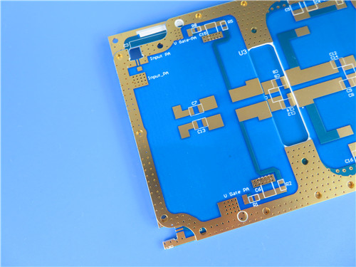
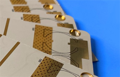
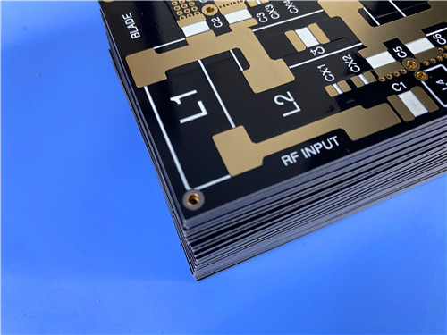
What Benefits Does a CuClad 250 PCB Bring to High-Frequency Circuit Design?


1.Introduction

High-frequency circuit design demands substrate materials that can maintain signal integrity across microwave and millimeter-wave bands. Among the various PTFE-based laminates available, Rogers CuClad 250 has established itself as a reliable option for engineers balancing electrical performance with mechanical robustness. Unlike pure PTFE substrates that can suffer from dimensional instability, CuClad 250 incorporates a cross-plied woven fiberglass reinforcement that bridges the gap between high-frequency performance and conventional PCB manufacturability.


For design teams working on radar frontends, microwave filters, or low-noise amplifiers (LNAs), selecting the right laminate directly impacts insertion loss, phase consistency, and long-term reliability. This article breaks down the material science behind CuClad 250, presents measured performance data, and walks through a real-world 2-layer board specification to illustrate how these properties translate into practical design outcomes.


2. Quick Answer

A CuClad 250 PCB delivers stable dielectric performance (Dk 2.40–2.55 at 10 GHz) with extremely low dissipation factor (0.0017), making it well-suited for microwave and radar applications where signal loss must be minimized. Its cross-plied woven fiberglass construction improves dimensional stability and mechanical strength compared to non-woven alternatives, while maintaining the low-loss characteristics expected from PTFE composites. The material supports standard PCB fabrication processes including immersion gold surface finish and 100% electrical testing, enabling production-grade high-frequency boards with IPC-Class-2 quality standards.


3.Key Takeaways


1) Consistent low Dk across frequencies: CuClad 250 maintains a dielectric constant of 2.40 to 2.55 from 1 MHz through 10 GHz, supporting wider transmission line widths and lower insertion loss for impedance-controlled designs.


2) Superior mechanical balance: Cross-plied fiberglass orientation (alternating 90°plies) delivers balanced electrical and mechanical properties in both X and Y axes, reducing warpage and improving dimensional stability.


3) Low loss for high-frequency bands: A dissipation factor of 0.0017 at 10 GHz ensures minimal signal attenuation, critical for radar, ECM, and ESM systems operating at microwave frequencies.


4) Environmental resilience: With 0.03% moisture absorption and near-zero outgassing (TML 0.01%, CVCM 0.0%), the material performs reliably in humid and vacuum environments.


5) Manufacturing compatibility: CuClad 250 supports standard PCB processing including 0.3 mm minimum drill sizes, 4/6 mil trace/space, and immersion gold surface finish, with IPC-Class-2 quality achievable in volume production.


4.Understanding CuClad 250 Material Composition


Rogers CuClad 250 is a composite laminate consisting of polytetrafluoroethylene (PTFE) resin reinforced with cross-plied woven fiberglass fabric. What distinguishes it from many other high-frequency substrates is its higher fiberglass-to-PTFE ratio, which shifts the material's mechanical profile closer to that of conventional FR-4 substrates while preserving the electrical benefits of PTFE.


The cross-plied construction means that alternating fiberglass plies are oriented at 90 degrees to each other. This layup strategy creates isotropic-like behavior in the planar directions. For designers, this translates to more predictable dielectric constant uniformity across the board area and reduced risk of skewed impedance values depending on trace orientation—a common concern with non-woven or unidirectionally reinforced PTFE laminates.


A standard 2-layer CuClad 250 stackup uses a 0.254 mm (10 mil) core with 35μm (1 oz) copper cladding on both sides. This configuration is particularly common for microwave component boards where controlled impedance and minimal dielectric thickness variation are required.


CuClad 250 PCB


5. Core Electrical Properties and Performance Data


5.1 Dielectric Constant Uniformity

The dielectric constant (Dk) of CuClad 250 ranges from 2.40 to 2.55, measured at both 1 MHz and 10 GHz. This tight tolerance is significant for two reasons. First, a lower Dk allows designers to use wider transmission lines for a given target impedance—typically 50 ohms in RF systems—which reduces conductor loss and eases manufacturing tolerances. For example, on a 10 mil thick CuClad 250 core, a 50-ohm microstrip line can be approximately 27 mils wide, compared to roughly 18 mils on a Dk 3.5 substrate. Wider traces are easier to etch consistently and suffer less from skin-effect losses at high frequencies.


Second, the stability of Dk across frequency bands ensures that impedance and phase response remain predictable as operating frequencies scale up. This is especially valuable for broadband components such as directional couplers and multi-octave filters.


5.2 Dissipation Factor and Insertion Loss

With a dissipation factor (Df) of just 0.0017 at 10 GHz, CuClad 250 ranks among the lower-loss commercially available PCB materials. To put this in perspective: conventional FR-4 materials typically exhibit Df values between 0.02 and 0.025 at similar frequencies, meaning CuClad 250 reduces dielectric loss by over an order of magnitude. For a 10 cm transmission line at 10 GHz, this difference can translate to several decibels of saved signal power—often the margin between meeting or failing system noise figure requirements.


5.3 Peel Strength

Copper peel strength of 14 lbs/in indicates robust adhesion between the copper foil and the PTFE-fiberglass substrate. This is an important reliability metric, particularly for boards that undergo thermal cycling or operate in mechanically demanding environments. Higher peel strength reduces the risk of trace lifting during assembly reflow or field operation.


6.Mechanical and Environmental Reliability


6.1 Dimensional Stability

The cross-plied woven fiberglass structure gives CuClad 250 better dimensional stability and lower thermal expansion in all directions compared to non-woven PTFE laminates. For PCB fabricators, this means tighter registration tolerance between layers and more predictable etch factor. For end users, it translates to consistent board dimensions across temperature excursions, which matters for antenna arrays and phased array radar systems where element spacing directly affects beam steering accuracy.


6.2 Moisture Absorption

At 0.03% moisture absorption, CuClad 250 is highly resistant to humidity-induced performance drift. Because water has a much higher dielectric constant (~80), even small amounts of absorbed moisture can measurably shift a substrate's effective Dk and increase loss. The 0.03% figure ensures that boards deployed in outdoor or high-humidity environments maintain their designed electrical characteristics without extensive conformal coating requirements.


6.3 Outgassing Performance

For aerospace and vacuum applications, outgassing is a critical selection criterion. CuClad 250 reports a Total Mass Loss (TML) of just 0.01%, Collected Volatile Condensable Material (CVCM) of 0.0%, and 0% Water Vapor Regain (WVR). These values meet or exceed typical space-grade material requirements, making the laminate suitable for satellite communications payloads and high-vacuum test equipment.


7. Real-World Application: 2-Layer CuClad 250 PCB Specification

To illustrate how these material properties translate into a production board, consider a recently fabricated2-layer rigid CuClad 250 PCB designed for a microwave subsystem.


7.1 Board Profile


  • Dimensions: 48.6 mm×76.9 mm (single panel), tolerance±0.15 mm
  • Finished thickness: 0.4 mm
  • Copper weight: 1 oz (35μm / 1.4 mils) on outer layers
  • Via plating thickness: 20μm minimum
  • Surface finish: Immersion Gold (ENIG)
  • Solder mask: Blue on top side only
  • Silkscreen: White on top side only


7.2 Fabrication Standards


  • Minimum trace/space: 4/6 mils
  • Minimum hole size: 0.3 mm
  • Quality standard: IPC-Class-2
  • 100% electrical test prior to shipment
  • Artwork format: Gerber RS-274-X


This particular board demonstrates several practical points. First, the 0.4 mm finished thickness (10 mil core + two copper layers) supports compact microwave assemblies where board height is constrained. Second, the use of immersion gold surface finish provides excellent RF contact performance and solderability for both SMT and through-hole components. Third, despite being a high-frequency PTFE-based material, CuClad 250 supports standard 0.3 mm drill sizes and 4/6 mil trace geometries—no specialized fabrication equipment is required beyond what a standard PCB shop already operates.


The absence of blind vias and the use of a simple 2-layer stackup also keep costs manageable, making CuClad 250 accessible for both prototyping and mid-volume production runs. Worldwide availability further supports global supply chains for OEMs building radar, electronic countermeasure (ECM), and electronic support measure (ESM) systems.


Typical Applications and Use Cases


CuClad 250 high frequency PCBs find their strongest fit in applications where low loss and dielectric consistency directly determine system performance:


  • Radar systems: Both transmit and receive frontends benefit from low insertion loss and stable Dk across temperature and frequency.


  • Electronic Countermeasures (ECM) and Electronic Support Measures (ESM): Broadband performance and signal fidelity are essential for signal intelligence and jamming systems.


  • Microwave components: Low-noise amplifiers (LNAs), filters, directional couplers, power dividers, and hybrid couplers all leverage the material's controlled impedance and low-loss properties.


  • Aerospace and satellite communications: The low-outgassing characteristics support vacuum and near-vacuum operating environments.


FAQ


Q1: How does CuClad 250 compare to RO4000 series materials for high-frequency designs?


CuClad 250 generally offers a lower Dk (2.4–2.55 vs. ~3.5 for RO4003C) and lower dissipation factor, resulting in wider transmission lines and lower dielectric loss. RO4000 series materials often provide higher glass transition temperature and may be preferred for higher-power or higher-temperature applications. The choice depends on whether the design prioritizes lowest possible loss or thermal robustness.


Q2: Can CuClad 250 PCBs be fabricated using standard FR-4 manufacturing processes?


Yes, for the most part. CuClad 250 supports standard drilling, etching, and plating processes. The 0.3 mm minimum hole size and 4/6 mil trace/space achievable on CuClad 250 align with standard PCB shop capabilities. However, PTFE-based materials do require specific surface preparation for plating adhesion, and experienced high-frequency PCB fabricators typically have established processes for these materials.


Q3: What is the typical impedance tolerance for CuClad 250 microstrip lines?


With controlled dielectric thickness and consistent Dk uniformity, impedance tolerances of±10% are standard, and±5% is achievable with tight process controls. The cross-plied fiberglass structure helps reduce Dk variation across the panel, contributing to more consistent impedance values compared to non-woven PTFE substrates.


Q4: Is CuClad 250 suitable for multilayer PCB designs?


While CuClad 250 is most commonly used in 2-layer configurations for simple microwave circuits, it can be incorporated into multilayer stackups when bonded with appropriate prepreg materials. However, multilayer designs with PTFE cores require careful material matching and lamination process control. For complex multilayer high-frequency designs, consulting with the PCB fabricator early in the design phase is recommended.


Conclusion

CuClad 250 occupies a valuable niche in the high-frequency PCB material landscape, combining the low-loss electrical performance of PTFE with the mechanical reliability of woven fiberglass reinforcement. Its Dk of 2.40–2.55 at 10 GHz, dissipation factor of 0.0017, and strong peel strength make it a practical choice for microwave components, radar frontends, and aerospace systems where both signal integrity and mechanical durability matter.


The real-world 2-layer board example demonstrates that these material properties translate directly into producible designs—supporting standard feature sizes, immersion gold surface finish, and IPC-Class-2 quality standards without requiring exotic fabrication techniques. For design engineers evaluating substrate options for their next high-frequency project, CuClad 250 deserves consideration as a balanced, production-ready material that does not force a tradeoff between electrical performance and manufacturability.


What Is WL-CT300 PCB? A Practical Guide to Low-Loss RF Substrates


WL-CT300 PCB is a thermosetting high-frequency laminate from Wangling WL-CT series, composed of hydrocarbon resin, ceramic filler, and fiberglass cloth reinforcement. With a dielectric constant (Dk) of 3.00 and dissipation factor (Df) of 0.0025 at 10 GHz, it delivers FR-4-like manufacturability with performance approaching premium PTFE-based materials. It is widely used in base station antennas, automotive radar, power amplifiers, and satellite communication systems where low loss, thermal stability, and production yield are equally important.


Key Takeaways

  • Dk = 3.00, Df = 0.0025 at 10 GHz—significantly lower loss than FR-4 (Df ~0.02), with performance comparable to mid-range PTFE laminates.
  • FR-4-compatible processing—no plasma treatment or special drilling required, resulting in higher fabrication yields and lower prototyping costs than PTFE.
  • Excellent thermal stability—TCDK of 27 ppm/°C and Tg above 280°C ensure consistent performance across temperature extremes.
  • CTE closely matched to copper—15 ppm/°C in X-axis and 14 ppm/°C in Y-axis reduce plated through-hole fatigue and improve long-term reliability
  • Cost-effective alternative—can substitute for imported high-frequency laminates like Rogers RO4000 series in many applications without major design changes.


1. Why Low-Loss Materials Matter in Modern RF Design


  • As wireless communication systems push toward higher frequencies—5G massive MIMO, 77 GHz automotive radar, Ku-band satellite links—every decibel of insertion loss matters. A 0.5 dB loss in a feed network might seem negligible on paper, but in a 64-element phased array, it compounds into a 3 dB reduction in effective radiated power. That is the difference between hitting your link budget and falling short.
  • For decades, engineers have faced a difficult choice: use FR-4 and accept high loss, or switch to PTFE-based laminates and pay the price in manufacturing complexity. PTFE materials deliver excellent electrical performance, but they are notoriously difficult to fabricate. They require special drill bits, plasma treatment for via adhesion, and carefully controlled lamination cycles. Treat a PTFE board like FR-4, and you end up with delamination, poor plating adhesion, and yield rates that can drop below 50%.
  • WL-CT300 was developed to bridge this gap. It offers the electrical performance needed for GHz-range designs while maintaining a processing workflow that is nearly identical to standard FR-4. For many applications, this balance of performance and manufacturability makes it the most practical choice on the market.


2. What Is WL-CT300 PCB? Material Composition Explained


WL-CT300 is part of Wangling's WL-CT series of organic polymer ceramic fiberglass cloth copper-clad laminates. Unlike PTFE-based materials that rely on polytetrafluoroethylene as the resin matrix, WL-CT300 uses a hydrocarbon resin system filled with ceramic particles and reinforced with woven fiberglass cloth.


This three-component system is carefully engineered:


-Hydrocarbon resin provides the base dielectric matrix with inherently low loss characteristics. Unlike epoxy-based FR-4 resins that have polar molecules that absorb electromagnetic energy, hydrocarbon resins are non-polar, resulting in much lower dissipation at high frequencies.

Ceramic filler is added to fine-tune the dielectric constant and improve thermal conductivity. The ceramic particles also enhance dimensional stability and reduce the coefficient of thermal expansion.


-Fiberglass cloth reinforcement provides mechanical strength and structural rigidity, similar to FR-4. This is what gives WL-CT300 its familiar handling characteristics and makes it compatible with standard PCB fabrication equipment.


-WL-CT300 is the Dk 3.00 variant in a broader family that includes Dk values of 3.30, 3.38, 3.48, 4.10, and 6.15. This range allows engineers to select the exact Dk that matches their impedance and design requirements, rather than being forced to compromise.


WL-CT300 PCB


3. Core Electrical and Mechanical Properties (With Data)

Numbers only matter if you understand what they mean for your design. Here is a breakdown of WL-CT300's key specifications and their practical implications.


Parameter

Value

Engineering Significance

Dielectric Constant (Dk) @ 10 GHz / 23°C

3.00 ± 0.05

Low Dk enables wider transmission lines for a given impedance, reducing conductor loss and improving manufacturing tolerance

Dissipation Factor (Df) @ 10 GHz

0.0025

~8–10× lower loss than standard FR-4 (Df 0.02); comparable to Rogers RO4003C (Df 0.0027)

Thermal Coefficient of Dk (TCDK)

27 ppm/°C

Dk changes by only 0.00081 per 10°C — critical for filter and oscillator frequency stability

Glass Transition Temperature (Tg)

> 280°C

Far above standard FR-4 (Tg ~130–180°C); ensures dimensional stability during lead-free reflow

Thermal Conductivity

0.41 W/mK

~30% higher than standard FR-4 (~0.3 W/mK); improves heat dissipation in power amplifier designs

Moisture Absorption

0.15%

Very low moisture uptake prevents Dk drift in humid environments — essential for outdoor base station equipment

CTE (X / Y / Z-axis)

15 / 14 / 31 ppm/°C

X/Y CTE closely matches copper (17 ppm/°C), minimizing stress on plated through-holes during thermal cycling


To put the loss numbers in perspective: a 100 mm microstrip transmission line on FR-4 at 10 GHz would have approximately 1.5–2.0 dB of dielectric loss. The same line on WL-CT300 would have only 0.15–0.25 dB. That is an order of magnitude improvement, and it directly translates to better receiver sensitivity, higher transmitter efficiency, and lower thermal load.


4. WL-CT300 vs. Common Alternatives

Understanding how WL-CT300 compares to other materials helps you make the right selection.


  • WL-CT300 vs. Standard FR-4

FR-4 is cheap and widely available, but its loss becomes unacceptable above 1–2 GHz for most RF applications. WL-CT300 offers dramatically lower Df, better thermal stability, and tighter Dk tolerance. The trade-off is cost—WL-CT300 is more expensive than FR-4, but still far more affordable than premium PTFE laminates.


  • WL-CT300 vs. PTFE-Based Laminates (Rogers RO4000 Series)

PTFE materials like Rogers RO4003C (Dk 3.38, Df 0.0027) have set the standard for high-frequency PCBs. However, they are expensive and difficult to manufacture. WL-CT300 offers similar electrical performance with a key advantage: it processes like FR-4. No plasma treatment, no special drill bits, no sodium naphthalene etching. This means faster turnaround times, higher yields, and lower fabrication costs—especially for prototypes and small-to-medium production runs.


  • WL-CT300 vs. Other Hydrocarbon Ceramics

WL-CT300 is part of a growing category of hydrocarbon ceramic laminates that includes materials like Isola IS680 and Panasonic Megtron6. What sets WL-CT300 apart is its combination of very low Dk (3.00), excellent Df (0.0025), and competitive pricing—particularly for customers in Asia who benefit from local manufacturing and shorter supply chains.


5. Real-World Applications and Design Cases

WL-CT300's balance of performance and manufacturability makes it suitable for a wide range of high-frequency applications.


5.1 Base Station Antennas and DAS

In 4G and 5G base station antennas, feed networks and power dividers must maintain consistent performance across temperature and humidity. WL-CT300's low TCDK (27 ppm/°C) and low moisture absorption (0.15%) ensure that antenna boresight and sidelobe levels stay within specification from–40°C to +85°C. The FR-4-like processing also means antenna manufacturers can use their existing PCB supply chain without retraining.


5.2 Automotive Radar and ADAS Sensors

77 GHz automotive radar modules demand extremely stable dielectric properties because even a tiny Dk shift can move the target detection range. WL-CT300's tight Dk tolerance (±0.05) and excellent thermal stability make it well-suited for radar feed networks and antenna arrays. Its high Tg (>280°C) also withstands the multiple reflow cycles common in automotive assembly.


5.3 Power Amplifiers and RF Modules

Power amplifiers generate significant heat, and thermal management is critical. WL-CT300's thermal conductivity of 0.41 W/mK—about 30% better than FR-4—helps spread heat away from active devices. Combined with its low loss, which reduces the amount of heat generated in the substrate itself, it is a practical choice for medium-power amplifier designs.


5.4 Satellite Communication and LNBs

Low-noise block downconverters (LNBs) and satellite receiver front-ends require low loss and stable Dk to maintain signal-to-noise ratio. WL-CT300's Df of 0.0025 at 10 GHz ensures minimal insertion loss in the RF front-end, while its stable TCDK prevents frequency drift as the dish heats up in direct sunlight.


6. Fabrication Insights: What We've Learned from Production

As a PCB fabricator with years of experience processing WL-CT series materials, we have gathered practical insights that are not always in the datasheet.


-Drilling: Standard carbide drills work perfectly. No special tooling is needed, unlike PTFE which often requires diamond-coated or high-helix drills. Feed and speed parameters are nearly identical to FR-4.

-Plating: Standard electroless copper + electroplating achieves reliable via adhesion. No plasma treatment or chemical etching is required to activate the dielectric surface—this is the single biggest manufacturing advantage over PTFE.


-Lamination: WL-CT300 is a thermoset material, so it uses standard lamination profiles. For multilayer designs, matching prepreg is available from Wangling, making it straightforward to build hybrid stacks with FR-4 layers for digital sections.


-Solder Mask: Standard liquid photoimageable solder mask adheres well to WL-CT300. This is another advantage over PTFE, where solder mask adhesion can be problematic.


-Copper Foil Options: WL-CT300 is available with standard ED copper or reverse-treated RTF copper. For applications requiring low passive intermodulation (PIM)—such as base station antennas—RTF copper is recommended because its smoother surface reduces conductor loss and PIM distortion.


7. When to Choose WL-CT300 (and When Not To)

WL-CT300 high frequency PCB is an excellent material, but it is not the best choice for every application.


Choose WL-CT300 when:

  • You need better performance than FR-4 but cannot justify PTFE pricing
  • Your design operates between 1 GHz and 15 GHz
  • Manufacturing yield and prototyping speed are priorities
  • You need multilayer capability with standard lamination processes
  • Your application requires consistent performance across temperature and humidity


Consider alternatives when:

  • You need Dk values below 3.0 (consider pure PTFE materials like Rogers RO3003, Dk 3.0 or lower)
  • You are designing above 30 GHz where PTFE's lower loss becomes more critical
  • Your application requires the absolute lowest possible Df regardless of cost
  • You need ultra-thin substrates below 0.1 mm where PTFE films may be more available


8. Frequently Asked Questions (FAQ)


Q: Is WL-CT300 the same as Rogers RO4003C?

A: No, they are different materials from different manufacturers. WL-CT300 has a Dk of 3.00 while RO4003C is 3.38. Their Df values are similar (0.0025 vs. 0.0027 at 10 GHz). WL-CT300 uses hydrocarbon resin, while RO4003C uses ceramic-filled PTFE. They are not drop-in replacements, but many designs can be adapted from one to the other with minor impedance adjustments.


Q: Can WL-CT300 be used in multilayer PCBs?

A: Yes, WL-CT300 is suitable for multilayer designs. Wangling provides matching prepreg materials, and the thermosetting resin system is compatible with standard lamination processes. It is common to see hybrid stacks with WL-CT300 for RF layers and FR-4 for digital control layers.


Q: Does WL-CT300 meet IPC standards?

A: Yes, WL-CT300 PCBs are fabricated to IPC-6012 Class 2 or Class 3 standards as required. The material itself is UL recognized and RoHS compliant.


Q: How does the cost of WL-CT300 compare to other high-frequency materials?

A: As a general rule, WL-CT300 is priced significantly lower than premium imported PTFE laminates like the Rogers 4000 series. The exact savings depend on board size, layer count, and volume, but reductions of 30–50% in material cost are not uncommon.


Final Thoughts


WL-CT300 occupies an important sweet spot in the high-frequency PCB material landscape. It delivers genuinely useful RF performance—Dk 3.00, Df 0.0025 at 10 GHz—in a package that processes like standard FR-4. For engineers working on base station antennas, automotive radar, power amplifiers, or satellite receivers, this combination is often exactly what is needed: good enough performance to meet the spec, and manufacturable enough to hit the cost target.


The key insight is that "best" is not always the same as "highest performance." In real-world engineering, the best material is the one that delivers the required performance at the lowest total cost—including fabrication yield, assembly reliability, and supply chain risk. By that measure, Wangling WL-CT300 is a strong contender for a wide range of high-frequency designs.


What Makes F4BTD350S PCB the Right Choice for High-Power RF Designs?


Quick Answer

The F4BTD350S PCB is a PTFE-based high-frequency circuit board engineered explicitly for high-power radio frequency (RF) and microwave applications where thermal management and signal integrity are non-negotiable. Built on a glass-fiber-reinforced PTFE substrate loaded with high-thermal-conductivity ceramic fillers, it delivers a stable dielectric constant of 3.5 at 10 GHz, an ultra-low dissipation factor of 0.0016, and a thermal conductivity of 1.25 W/m·K—a combination that outperforms standard FR-4 and many mid-tier high-frequency laminates in power-handling capacity and long-term reliability. For engineers designing power amplifiers, antenna feeds, industrial heating systems, or passive components such as couplers and filters, the F4BTD350S substrate reduces insertion loss, improves heat dissipation, and lowers the risk of thermal failure under continuous high-temperature operation.


Key Takeaways


1) Superior thermal performance for power-dense RF:

With 1.25 W/m·K thermal conductivity—roughly three to four times that of conventional FR-4—F4BTD350S PCBs spread heat more evenly across the board, extending component life in power amplifiers and industrial heating equipment.


2) Exceptionally low loss at microwave frequencies:

A dissipation factor of 0.0016 at 10 GHz means less signal energy is converted to heat, preserving output power and reducing thermal load in high-frequency transmit chains.


3) Stable dielectric across temperature and frequency:

Dk of 3.5±0.07 at 10 GHz and a thermal coefficient of Dk of only−45 ppm/°C ensure consistent impedance matching and filter response from−55°C to 150°C.


4) Mechanically robust for manufacturability:

Low CTE in the x/y plane (11/10 ppm/°C) and UL-94 V0 flammability rating improve through-hole reliability, dimensional stability during assembly, and overall safety compliance.


5) Versatile across high-power RF segments:

From base-station power amplifiers and phased-array antennas to RF couplers, power splitters, and industrial microwave heating systems, F4BTD350S covers a wide range of applications where both power handling and low loss matter.


Understanding F4BTD350S: Beyond the Datasheet Numbers

When engineers evaluate high-frequency PCB materials, they often start and end with Dk and Df values. But in high-power RF designs, those two numbers tell only a fraction of the story. What ultimately determines whether a board survives years of continuous operation—and whether it meets regulatory and performance targets—is how the material behaves under combined thermal, electrical, and mechanical stress. This is where F4BTD350S distinguishes itself from commodity PTFE boards and even from some better-known branded alternatives.


Wangling F4BTD350S is a PTFE (polytetrafluoroethylene) resin system reinforced with woven glass fiber and heavily loaded with specialized high-thermal-conductivity ceramic particles. The glass-fiber weave provides mechanical rigidity and dimensional stability, which pure PTFE alone cannot offer. The ceramic filler is the real differentiator: it raises thermal conductivity from the 0.3–0.5 W/m·K range typical of standard PTFE substrates to 1.25 W/m·K. That jump is not incremental—it fundamentally changes how heat generated by power transistors, RF power dividers, or microwave heating elements moves away from the source and into the surrounding structure or heat sink.


For a practical 2-layer F4BTD350S PCB built with 1 oz copper on both sides and a 0.508 mm core, the thermal path from a top-side power device to a bottom-side heat spreader is significantly more efficient than an equivalent FR-4 or standard PTFE board. In power amplifier designs, this translates directly to lower junction temperatures at the same output power, or alternatively, higher achievable output power before derating is required. Field experience from RF manufacturing teams shows that power amplifiers built on high-thermal-conductivity PTFE substrates typically run 15–25°C cooler at the transistor base than comparable units on standard low-loss laminates, depending on power level and airflow.


F4BTD350S PCB


Electrical Performance: Why 0.0016 Dissipation Factor Matters in Practice

Loss in an RF PCB comes from multiple sources—conductor loss, dielectric loss, radiation loss, and leakage. At frequencies above 1 GHz, dielectric loss becomes a significant contributor, and at microwave bands (3–30 GHz), it often dominates the total insertion budget. The dissipation factor (Df) of 0.0016 at 10 GHz places F4BTD350S firmly in the low-loss category, well below the 0.01–0.02 range of FR-4 and even below many mid-range hydrocarbon-ceramic laminates.


Why does this matter beyond the lab bench? In a transmit chain, every decibel lost in the substrate is a decibel that the power amplifier must produce extra—and that extra power turns into heat. Over the lifetime of a base-station amplifier or an industrial microwave generator, those extra watts accumulate into higher energy consumption, more thermal cycling, and shorter component life. For filter and coupler designs, low Df directly translates to sharper roll-off, deeper stop-band rejection, and lower insertion loss in the pass-band, which simplifies system-level tuning and reduces the need for gain compensation stages.


Equally important is dielectric stability. F4BTD350S maintains a Dk of 3.5 with a tolerance of±0.07 across the panel and a thermal coefficient of Dk (TCDk) of−45 ppm/°C from−55°C to 150°C. For precision filters and tightly matched antenna feeds, even a small drift in Dk can shift the center frequency enough to push the design out of specification. The low TCDk of F4BTD350S means that a filter tuned at room temperature will stay within its pass-band window across the full operating temperature range, reducing the need for active compensation or over-design.


Mechanical and Thermal Reliability: The Manufacturing Perspective

One of the less discussed but critical advantages of F4BTD350S is its dimensional stability, driven by a low coefficient of thermal expansion (CTE). In the x-axis, CTE is 11 ppm/°C; in the y-axis, 10 ppm/°C; and in the z-axis, 40 ppm/°C, measured from−55°C to 288°C. The in-plane values are close to that of copper itself (around 17 ppm/°C), which greatly reduces shear stress on copper traces, plated through-holes, and solder joints during thermal cycling.


For PCB fabricators, this has real manufacturing implications. Plated through-holes (PTH) onF4BTD350S boards —even with a finished board thickness of only 0.6 mm and a 20μm copper plating thickness—show consistently higher reliability under thermal shock testing compared to higher-CTE PTFE materials. The glass-fiber reinforcement also improves drillability and reduces smear, resulting in cleaner hole walls and more consistent plating coverage. From a quality-control standpoint, boards built to IPC-Class-2 standards on F4BTD350S routinely pass electrical testing at 100% yield when proper drilling and plating parameters are used.


The material also carries a UL-94 V0 flammability rating and a Comparative Tracking Index (CTI) of 600 V, which simplifies compliance for industrial and telecom end-products. Moisture absorption is≤0.05%, another important parameter for outdoor and high-humidity deployments such as antenna arrays and remote radio units. Low moisture uptake prevents Dk drift, avoids delamination under reflow, and maintains insulation resistance over time—all factors that contribute to long field life with minimal maintenance.


Real-World Applications and Case Experience

F4BTD350S has found its strongest adoption in four application categories, each leveraging a different combination of the material's properties.


1) High-power RF power amplifiers (PAs) are the most common use case. Here, the 1.25 W/m·K thermal conductivity is the primary driver. In L-band and S-band power amplifiers for cellular infrastructure, public safety radio, and radar systems, designers often pair F4BTD350S with thick copper cladding (1 oz or higher) and backside thermal vias to create an efficient heat path from transistor packages to the chassis. Production data from contract manufacturers shows that PA modules on F4BTD350S substrates exhibit lower rates of field returns related to thermal fatigue compared to previous-generation boards using standard PTFE.


2) Antenna feed networks and phased-array elements benefit from the combination of stable Dk, low loss, and low CTE. In array antennas where hundreds or thousands of elements must be phase-matched, board-to-board Dk consistency and temperature stability directly impact beam-pointing accuracy and side-lobe levels. The±0.07 Dk tolerance of F4BTD350S supports tight element-to-element matching without the need for per-board trimming in many designs.

Passive RF components—couplers, filters, and power splitters—are another major segment. For these parts, insertion loss, isolation, and return loss are the key performance metrics, and all three improve when the substrate has low Df and controlled Dk. Manufacturers of directional couplers for test and measurement equipment frequently switch to F4BTD350S when their standard substrate can no longer meet loss targets at higher frequency bands.


3) Industrial heating and microwave processing equipment represent a more specialized but growing application. In these systems, the board itself may carry very high RF power levels and operate in elevated ambient temperatures. The high thermal conductivity, UL-94 V0 rating, and ability to withstand continuous operation at high temperatures make F4BTD350S a natural fit where FR-4 and even some standard PTFE materials would degrade prematurely.


Data Comparison: F4BTD350S Against Common Alternatives

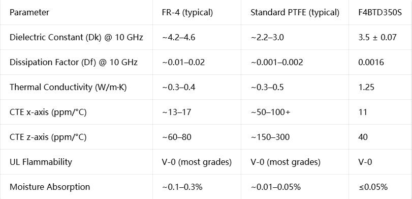
To put F4BTD350S performance in context, it is useful to compare its core parameters against two widely used reference materials: standard FR-4 and a typical mid-range PTFE microwave substrate.


Data Comparison: F4BTD350S Against Common Alternatives


The data shows that F4BTD350S occupies a unique position: it offers the low loss expected from a PTFE-based material while delivering thermal conductivity and in-plane dimensional stability closer to what would normally require a much more expensive specialty ceramic-filled composite. For designs that need both low insertion loss and effective heat dissipation—which is the case for nearly all high-power RF applications—F4BTD350S provides a compelling balance of performance and manufacturability.


Manufacturing Specifications in Context

A representative double-sided F4BTD350S PCB for RF applications might be built with the following parameters, all of which are well within standard fabrication capabilities for experienced high-frequency PCB shops:


  • Board thickness: 0.6 mm finished, with a0.508 mm F4BTD350S core and 35μm (1 oz) copper on both layers
  • Minimum trace/space: 7/9 mils, achievable with standard etching processes on 1 oz copper
  • Minimum drilled hole: 0.6 mm, with 20μm via plating thickness meeting IPC-Class-2 requirements
  • Surface finish: Immersion gold (ENIG), preferred for RF boards because of its flat surface, consistent contact resistance, and solderability
  • Solder mask and silkscreen: Black solder mask on the top side for contrast and light absorption, with white silkscreen for component reference designators
  • Quality control: 100% electrical testing before shipment, verifying continuity and isolation on all nets


These specifications are not extreme or exotic—and that is part of the value proposition. F4BTD350S does not require specialized non-standard processing that would drive up cost or lead time. A competent PCB fabricator experienced with PTFE materials can produce F4BTD350S boards using standard drill bits, plating lines, and lamination cycles, as long as they follow proper PTFE surface preparation for adhesion.


Frequently Asked Questions (FAQ)


Q: Is F4BTD350S suitable for multilayer PCBs, or only 2-layer designs?

A: F4BTD350S is suitable for multilayer and high-layer-count designs, including backplanes. The material's good mechanical properties and dimensional stability support reliable lamination and registration in multilayer stacks. That said, many high-power RF applications that use F4BTD350S are implemented as 2-layer or 4-layer boards because the power devices and transmission lines are often placed on the outer layers for thermal and RF performance reasons.


Q: How does F4BTD350S compare to Rogers RO4000 series materials?

A: Both are ceramic-filled PTFE composites targeting high-frequency applications, and both offer low loss and good thermal performance relative to FR-4. F4BTD350S is positioned as a high-thermal-conductivity option with Dk 3.5 and 1.25 W/m·K thermal conductivity. When selecting between materials, engineers should compare specific grade parameters (Dk, Df, thermal conductivity, CTE), availability, and total cost of fabrication for their specific design rather than relying on brand alone.


Q: Can F4BTD350S PCBs be assembled with standard SMT reflow processes?

A: Yes. F4BTD350S is compatible with standard SMT assembly, including lead-free reflow profiles. Its UL-94 V0 rating, low CTE, and low moisture absorption contribute to reliable soldering and reduce the risk of delamination or pad lifting during reflow. As with any PTFE-based material, proper surface treatment before soldermask and surface-finish application is important for adhesion.


Q: What is the typical lead time for F4BTD350S PCB prototypes?

A: For standard 2-layer F4BTD350S PCBs with common parameters (0.6 mm thickness, 1 oz copper, immersion gold, 0.6 mm minimum hole), prototype lead times are typically in the range of standard high-frequency board fabrication—usually a few weeks depending on panel size, quantity, and testing requirements. Worldwide shipping is available from qualified manufacturers.


Q: Does F4BTD350S meet IPC standards?

A: F4BTD350S PCBs can be manufactured and tested to IPC-Class-2 standards, which is the most common class for commercial and industrial electronic assemblies. Higher classes can be discussed on a case-by-case basis depending on the specific reliability and testing requirements of the end application.


Closing Thoughts

Selecting the right substrate for a high-power RF design is always a trade-off between electrical performance, thermal management, mechanical reliability, and cost. F4BTD350S stands out because it addresses the thermal bottleneck that plagues so many power-amplifier and industrial-microwave designs—without sacrificing the low-loss and stable-dielectric properties expected from a premium PTFE material. For engineers who have been pushing standard PTFE or FR-4 boards to their thermal limits, migrating to F4BTD350S often yields measurable improvements in operating temperature, component longevity, and overall system reliability. As with any material change, validating with a prototype build and thermal characterization under real operating conditions is always recommended—but for a growing number of high-power RF applications, F4BTD350S has become the default starting point rather than an exotic upgrade.


What Makes WL-CT350 PCB the Right Material for Modern High-Frequency RF Designs?


Quick Answer


WL-CT350 PCB is a hydrocarbon-ceramic fiberglass-reinforced high-frequency circuit board material manufactured by Wangling. Designed as a thermosetting resin-based alternative to PTFE substrates, it delivers a dielectric constant of 3.48 and dissipation factor of 0.0039 at 10 GHz, combined with a Tg above 280°C and FR4-like processability. Its low TCDK (52 ppm/°C), closely copper-matched CTE, and 0.7 W/m·K thermal conductivity make it suitable for base station antennas, automotive radar, power amplifiers, and RF filters where signal stability and thermal reliability matter. Unlike PTFE materials, Wangling WL-CT350 can be fabricated using standard PCB manufacturing flows, reducing cost and lead time while maintaining consistent circuit performance.


Key Takeaways


- Low-loss high-frequency performance: Dk 3.48 and Df 0.0039 at 10 GHz support reliable signal transmission across RF and microwave bands.


- FR4-compatible manufacturing: Hydrocarbon-thermoset chemistry enables standard PCB processing, unlike PTFE which requires specialized fabrication techniques.


- Exceptional thermal stability: Tg > 280°C and TCDK of 52 ppm/°C ensure consistent electrical properties across wide temperature ranges.


- Copper-matched CTE: X-axis 11 ppm/°C and Y-axis 14 ppm/°C minimize thermal stress on traces and plated vias, improving long-term reliability.


- Enhanced thermal management: Thermal conductivity of 0.7 W/m·K—roughly double standard FR4—aids heat dissipation in power-dense RF designs.


- Low moisture absorption: 0.05% absorption rate preserves impedance stability in high-humidity outdoor environments.


- Domestic import substitute: Cost-effective alternative to imported high-frequency laminates with comparable electrical specifications.


---


Understanding WL-CT350: A High-Frequency Substrate Built for Manufacturability


When selecting materials for RF and microwave circuits, engineers traditionally face a tradeoff: premium PTFE-based substrates deliver excellent electrical performance but are expensive and difficult to manufacture, while standard FR4 is cheap and processable but loses signal integrity at higher frequencies. WL-CT350, developed by Wangling, addresses this gap through a carefully engineered hydrocarbon-ceramic composite that combines strong high-frequency characteristics with FR4-like fabrication compatibility.


Material Composition and Architecture


WL-CT350 substrate is classified as an organic polymer ceramic fiberglass cloth copper clad laminate (CCL). Its dielectric layer is built from three core constituents:


1. Hydrocarbon resin matrix—A thermosetting polymer system that forms the structural binder of the material. Unlike PTFE (a thermoplastic), hydrocarbon resins cure into a rigid, dimensionally stable structure that behaves predictably during standard PCB manufacturing operations.


2. Ceramic filler particles—Dispersed throughout the resin matrix, ceramic fillers precisely tune the dielectric constant, boost thermal conductivity, and improve the temperature stability of both Dk and Df.


3. Woven fiberglass reinforcement—Provides mechanical strength and dimensional stability, functioning the same way it does in conventional FR4 substrates.


This three-part formulation is what gives WL-CT350 its dual advantage: the hydrocarbon-ceramic blend delivers the low-loss electrical performance needed for high-frequency designs, while the fiberglass-reinforced thermoset structure preserves the manufacturability that PCB fabricators rely on.


Electrical Performance: Dk, Df, and Why They Matter


  • For any high-frequency substrate, the two defining electrical parameters are dielectric constant (Dk, also called relative permittivityεr) and dissipation factor (Df, or loss tangent tanδ).


  • WL-CT350 is specified with a dielectric constant of 3.48 at 10 GHz and 23°C. This mid-range Dk value is well-suited for many RF applications—low enough to support reasonable trace widths for 50Ωimpedance lines, high enough to enable some degree of circuit miniaturization compared to lower-Dk PTFE materials.


  • The dissipation factor of 0.0039 at 10 GHz indicates low dielectric loss. To put this in perspective, standard FR4 typically has a Df in the range of 0.02–0.03 at similar frequencies, meaning WL-CT350 reduces dielectric absorption loss by roughly 85–90%. This directly translates to lower insertion loss in transmission lines, higher efficiency in power amplifiers, and better noise figure in receiver front-ends.


  • Equally critical is the temperature coefficient of dielectric constant (TCDK), which quantifies how much Dk shifts with temperature. WL-CT350 achieves a TCDK of 52 ppm/°C. Over a 100°C operating range, this corresponds to a Dk variation of only ~0.018, or roughly 0.5% relative change. For frequency-sensitive circuits such as filters, couplers, and antenna arrays—where even small Dk shifts can detune the design—this level of stability is essential for maintaining performance across environmental conditions.


Thermal and Mechanical Reliability Characteristics


  • High-frequency electronics often operate in demanding thermal environments: outdoor telecom equipment exposed to seasonal temperature swings, automotive modules near engine compartments, and aerospace hardware subjected to rapid thermal cycling. WL-CT350 is engineered to maintain both electrical and mechanical integrity under these conditions.


  • Glass transition temperature (Tg) is the temperature at which a polymer substrate transitions from a rigid, glassy state to a softer, rubbery state. WL-CT350's Tg exceeds 280°C, far above the 130–180°C range of standard FR4 grades. This high Tg ensures the material retains its mechanical stiffness and dimensional stability during multiple lead-free reflow cycles (typically peaking at 250–260°C) and during continuous high-temperature operation.


  • Coefficient of thermal expansion (CTE) describes how much a material expands when heated. Mismatched CTE between the substrate and copper conductors is a primary cause of PCB failure—differential expansion creates shear stress that can crack solder joints, fracture traces, or pull plated-through holes apart. WL-CT350 addresses this with carefully engineered CTE values:


- X-axis: 11 ppm/°C

- Y-axis: 14 ppm/°C

- Z-axis: 34 ppm/°C


  • Copper has a CTE of approximately 17 ppm/°C, so the in-plane (X-Y) values of WL-CT350 are very closely matched. This minimizes shear stress at the copper-dielectric interface, which is particularly important for fine-line RF traces and high-reliability plated vias. The Z-axis CTE of 34 ppm/°C, while higher, is still favorable compared to many pure PTFE substrates, supporting good plated-through-hole reliability through thermal cycling.


  • Thermal conductivity of 0.7 W/m·K is another notable advantage. Standard FR4 typically conducts only 0.3–0.4 W/m·K, meaning WL-CT350 dissipates heat roughly twice as effectively. For power amplifier boards and other heat-generating RF circuits, this improved thermal conduction helps lower component operating temperatures, extending device lifespan and reducing performance drift from self-heating.


Moisture Resistance for Outdoor Deployments


  • Water has an extremely high dielectric constant (~80), so even trace amounts of moisture absorbed into a substrate can measurably shift Dk, increase Df, and degrade impedance matching. This is a particular concern for outdoor equipment such as base station antennas, which are exposed to rain, fog, and high humidity year-round.


  • WL-CT350 features a moisture absorption rate of just 0.05%, exceptionally low for a resin-based substrate. This means that even after prolonged exposure to humid conditions, the change in electrical properties remains minimal—an important property for maintaining antenna pattern consistency and filter center frequency accuracy in field-deployed equipment.


---


Practical Implementation: 2-Layer WL-CT350 Stackup and Manufacturing


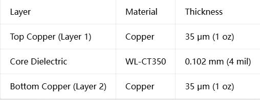
A typical2-layer WL-CT350 PCB configuration illustrates how the material translates into real-world designs. The standard stackup is straightforward:


2-Layer WL-CT350 Stackup


This 2-layer rigid configuration is commonly used for antenna feed networks, simple filter boards, and RF transmission line structures where controlled impedance microstrip lines are routed on the top layer with a solid ground plane on the bottom.


WL-CT350 PCB


Manufacturing Advantages Over PTFE


The manufacturability of WL-CT350 is one of its most significant differentiators from PTFE-based materials:


1) Drilling:

WL-CT350 drills cleanly with standard carbide tooling, producing well-defined hole walls with minimal burring. PTFE materials, by contrast, are soft and prone to smearing during drilling, often requiring specialized drill parameters and additional desmear or plasma etch steps to achieve reliable hole wall preparation for plating.


2) Plating and metallization:

The hydrocarbon resin surface accepts standard electroless copper deposition processes without special surface treatment, which is not the case for PTFE—PTFE's low surface energy typically requires sodium naphthalene etching or plasma treatment to achieve adequate copper adhesion.


3) Lamination and multilayer processing:

As a thermosetting material, WL-CT350 laminates predictably with matching prepreg materials, following lamination profiles similar to FR4. PTFE materials often require more complex lamination cycles with tighter pressure and temperature controls.


4) Dimensional stability:

The fiberglass reinforcement provides excellent dimensional stability during fabrication, ensuring that trace geometries and board dimensions remain consistent across production panels—an important factor for impedance-controlled RF boards.


Production files for WL-CT350 PCBs are supplied in standard Gerber RS-274-X format, and finished boards are typically inspected and tested to IPC-Class-2 acceptance standards, with 100% electrical testing performed before shipment. This adherence to industry-standard formats and specifications makes WL-CT350 easy to integrate into existing PCB procurement and quality assurance workflows.


---


Typical Application Areas


WL-CT350's combination of electrical performance, thermal stability, and manufacturing practicality makes it suitable for a broad range of high-frequency applications:


1) Base Station Antennas and Satellite Antennas—5G massive MIMO arrays and satellite communication antennas require consistent element-to-element performance across temperature extremes. WL-CT350's stable Dk and low loss ensure that each radiating element maintains its designed impedance and radiation characteristics.


2) Automotive Radar, Sensors, and Navigation Systems—Automotive radar modules (24 GHz and 77 GHz bands) must operate reliably from−40°C to +125°C while subjected to vibration and thermal cycling. The material's high Tg, matched CTE, and low TCDK align well with automotive reliability requirements.


3) Power Amplifiers—RF power amplifiers generate significant heat and benefit from WL-CT350's 0.7 W/m·K thermal conductivity. Stable Dk also ensures that impedance matching networks remain effective as the board temperature rises under load.


4) Satellite High-Frequency Heads (LNBs)—Low-noise block downconverters demand low-loss substrates at Ku-band frequencies. WL-CT350's low dissipation factor directly contributes to better system noise figure and reception sensitivity.


5) RF Devices and Filters—Filters and duplexers are highly sensitive to Dk variations. The 52 ppm/°C TCDK of WL-CT350 helps filter designs maintain their passband characteristics across operating temperature ranges.


6) WiMAX Antennas and Distributed Antenna Systems (DAS)—These infrastructure applications require cost-effective, volume-manufacturable substrates with consistent RF performance. WL-CT350's FR4-like processability supports high-volume production at a lower cost than PTFE alternatives.


---


Frequently Asked Questions (FAQ)


1) How does WL-CT350 compare to PTFE-based high-frequency substrates?


WL-CT350 generally has slightly higher loss than premium PTFE-ceramic materials but offers significantly better manufacturability and cost efficiency. PTFE substrates require specialized drilling, plasma surface treatment, and controlled lamination processes, all of which increase production cost and lead time. WL-CT350 processes with standard FR4-compatible workflows while still delivering strong high-frequency performance for most commercial RF applications.


2) Can WL-CT350 be used in multilayer PCB designs?


Yes. While the reference configuration in this article is a 2-layer stackup, WL-CT350 is available as a core material and can be used in multilayer constructions with compatible prepreg materials. It supports plated through-holes and can be integrated into mixed-dielectric stackups when combined with other material types.


3) Up to what frequency can WL-CT350 be used effectively?


WL-CT350 is characterized at 10 GHz and performs well through commonly used microwave bands including those for 5G sub-6 GHz, 24 GHz and 77 GHz automotive radar, and Ku-band satellite communications. Usability at higher frequencies depends on the specific design's loss budget and performance requirements.


4) Is WL-CT350 compatible with lead-free soldering processes?


Yes. With a Tg above 280°C, WL-CT350 comfortably withstands standard lead-free reflow profiles with peak temperatures around 250–260°C. The material is formulated to meet modern RoHS requirements and supports all common surface finishes including ENIG, lead-free HASL, OSP, and immersion silver.


5) What are the cost implications of choosing WL-CT350 versus imported alternatives?


WL-CT350 is positioned as a cost-competitive domestic alternative to imported high-frequency laminates. While pricing varies with volume, copper weight, and panel size, it typically provides meaningful cost savings compared to premium imported PTFE or hydrocarbon-ceramic materials, with comparable electrical performance for many commercial and industrial RF applications.


6) Does WL-CT350 require special storage or handling?


Standard PCB material storage practices apply—controlled temperature and humidity environments are recommended to prevent moisture uptake prior to fabrication. WL-CT350's low inherent moisture absorption rate (0.05%) makes it less sensitive to ambient conditions than some other high-frequency substrate materials.


---


Conclusion


WL-CT350 occupies a valuable position in the high-frequency PCB material landscape: it delivers the low-loss electrical performance and thermal stability that modern RF designs demand, while retaining the manufacturing simplicity and cost structure of conventional FR4-compatible materials. For engineers working on base station antennas, automotive radar, power amplifiers, filters, or satellite front-ends, it offers a practical balance of performance, reliability, and producibility.


As a domestically developed hydrocarbon-ceramic composite with well-characterized specifications and IPC-Class-2 compliance, WL-CT350 also provides supply chain resilience as a substitute for imported high-frequency laminates. Its combination of proven electrical data, thermal robustness, and manufacturing compatibility makes it a strong candidate for a wide range of current and next-generation RF and microwave PCB designs.


Traditional identification methods such as barcodes and printed labels often face limitations in large-scale management scenarios. RFID and NFC technologies provide a smarter alte


From inventory management and industrial asset tracking to textile management and digital product interaction, customized RFID and NFC solutions help companies optimize operations and improve overall efficiency.


Why RFID and NFC Technologies Are Widely Used in Modern Industries

RFID (Radio Frequency Identification) uses radio frequency signals to communicate between tags and readers. Unlike traditional labels that require direct scanning, RFID tags can be identified automatically without physical contact, making them ideal for high-volume tracking applications.


NFC (Near Field Communication) is a short-range wireless communication technology that allows quick data exchange between NFC tags and compatible devices such as smartphones.

Both technologies offer several advantages:

  • Fast and accurate identification
  • Reduced manual data entry
  • Improved inventory visibility
  • Better asset management efficiency
  • Flexible customization options

Due to these benefits, RFID and NFC products are widely used in manufacturing, logistics, healthcare, retail, hospitality, and supply chain industries.


Custom NFC Sticker Solutions for Smart Identification

As businesses increasingly adopt digital interaction solutions, NFC technology has become an effective way to connect physical products with digital information.


A custom NFC sticker for smart identification provides a flexible identification solution that can be attached to different surfaces, including products, packaging, equipment, and promotional materials.

By simply scanning the NFC tag with a smartphone, users can access product information, authentication details, digital content, or service platforms instantly.

Common applications include:

  • Product authentication and anti-counterfeiting
  • Smart packaging
  • Digital marketing interaction
  • Equipment identification
  • Information sharing

Compared with traditional labels, customized NFC stickers offer greater convenience and provide businesses with new opportunities to improve customer engagement and product management.


RFID Tags Improve Industrial Tracking and Asset Management

In industrial environments, accurate asset tracking is essential for improving productivity and reducing operational costs. RFID technology enables companies to monitor equipment, materials, and inventory throughout the entire management process.


Custom RFID tags can be designed according to different application requirements, including size, material, frequency, chip type, and environmental conditions.


Key benefits of RFID tracking solutions include:

  • Real-time asset monitoring
  • Faster inventory counting
  • Reduced tracking errors
  • Improved workflow efficiency
  • Better supply chain visibility

For industries with complex operating environments, reliable RFID solutions provide a practical way to build smarter and more efficient management systems.


Durable RFID Laundry Tag Solutions for Textile Management

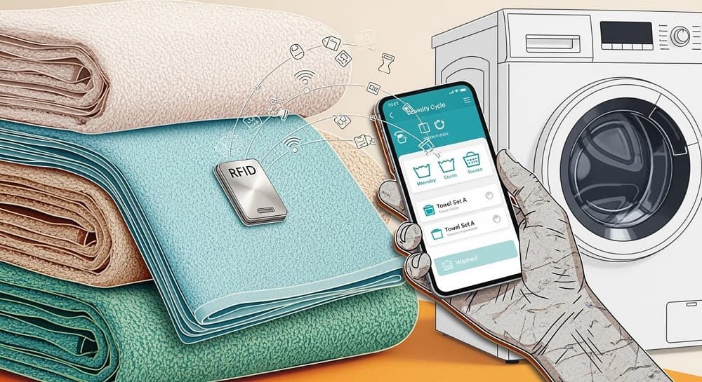
Hotels, hospitals, and commercial laundry companies often manage thousands of textile items every day. Traditional manual counting methods can easily lead to missing items, inaccurate records, and inefficient operations.


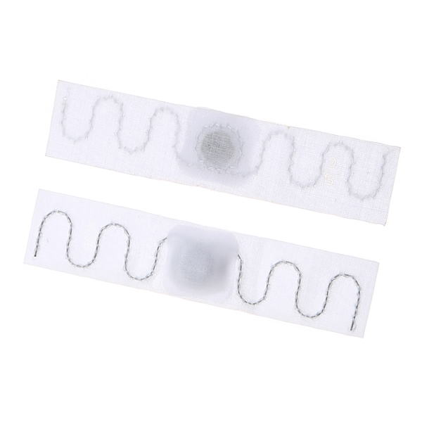
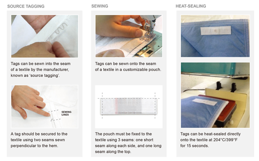
A durable RFID laundry tag for textile management is specially designed for textile tracking applications that require repeated washing and long-term durability. These RFID tags can withstand challenging laundry environments while maintaining stable identification performance. By attaching RFID tags to uniforms, towels, bedding, and other textile products, businesses can automatically track usage information and improve inventory control.


RFID laundry management systems help companies achieve:

  • Accurate textile tracking
  • Reduced item loss
  • Improved laundry efficiency
  • Better asset lifecycle management
  • Lower operational costs

With RFID technology, textile management becomes more transparent, automated, and reliable.


Industrial RFID Cable Tie Tag for Flexible Asset Tracking

Many industrial assets have irregular shapes or challenging installation conditions, making traditional identification labels difficult to apply. An industrial RFID cable tie tag for asset tracking provides a secure and convenient solution for identifying cables, pipes, equipment, containers, and other assets.


The cable tie design allows the RFID tag to be firmly attached to different objects, making it suitable for applications that require strong fixation and durability.


Typical applications include:

  • Cable management
  • Industrial equipment identification
  • Pipeline tracking
  • Logistics management
  • Outdoor asset monitoring


With waterproof materials and customizable designs, RFID cable tie tags can provide reliable performance even in demanding environments.


Customized RFID and NFC Solutions for Different Applications

Every business has unique identification requirements. Factors such as reading distance, working environment, installation method, and data storage capacity can affect the selection of RFID and NFC products.


Professional RFID manufacturers can provide customized solutions including:

  • Different RFID chip options
  • Various materials and sizes
  • Custom printing and encoding
  • Waterproof and durable designs
  • OEM and ODM services

By selecting the right RFID or NFC solution, businesses can improve operational efficiency and create more intelligent management systems.


RFID and NFC technologies are transforming the way businesses identify, track, and manage their products and assets. Whether for smart identification, industrial tracking, textile management, or specialized applications, customized RFID solutions provide businesses with greater accuracy, efficiency, and flexibility.


As industries continue moving toward digital transformation, RFID and NFC products will play an increasingly important role in improving automation and management efficiency. OEM RFID Factory provides customized RFID and NFC tag solutions for global customers, offering reliable products for asset tracking, smart identification, laundry management, and various industrial applications.


You see rapid growth in the radio frequency identification market for laundry in 2026. Sectors such as industrial laundries and healthcare now rely on advancements like the RFID laundry tags from SHENZHEN ZHIJIE IOT APPLICATION CO.LTD. This Nylon Textile UHF Laundry Tag delivers durability, efficiency, and cost-effectiveness. You gain real-time inventory management, precise loss control, and streamlined operations. With the Wholesale Price RFID UHF Laundry Tag, you secure a competitive edge and operational improvement in a changing industry.

Key Takeaways

  • RFID laundry tags are transforming the laundry industry by providing real-time inventory management and reducing manual labor.

  • Adoption rates for RFID technology are increasing in sectors like healthcare and hospitality, enhancing operational efficiency.

  • These tags automate processes, leading to significant cost savings and improved accuracy in inventory tracking.

  • Durable design ensures RFID tags withstand harsh laundry environments, maintaining functionality through numerous wash cycles.

  • Businesses can expect a return on investment within 12 to 18 months by reducing linen loss and labor costs.

  • Customization options allow businesses to tailor RFID tags to their specific needs, enhancing brand recognition and operational efficiency.

  • The integration of IoT with RFID technology improves traceability and inventory management, driving further adoption in the industry.

  • Future trends indicate continued growth in the RFID market, making it essential for businesses to adopt these technologies early for a competitive edge.

RFID Laundry Tag Trend in 2026

Adoption Rates

Industry Growth

You see the radio frequency identification market expanding rapidly in the laundry industry. RFID laundry tags now dominate high-volume applications. You notice commercial laundry operations and healthcare facilities adopting these tags at unprecedented rates. Market-leading performance drives this growth. You gain best-in-class performance with RFID laundry tags, which deliver reliable inventory tracking solutions for high-volume laundry environments. You experience real-time inventory management, which transforms asset visibility and management efficiency.

Leading Sectors

You observe industrial laundries, hospitality, and healthcare as the leading sectors for RFID laundry tag. Hospitals require precise tracking for linens and uniforms. Hotels use tags to manage large volumes of towels and bedding. Commercial laundry operations rely on RFID laundry tags to streamline sorting and reduce losses. You see these sectors investing in RFID technology to improve management and reduce manual labor. High-volume applications benefit most from RFID laundry tags, which provide accurate tracking and efficient management.

Drivers of RFID Laundry Tags

You drive operational improvement by adopting RFID laundry tags. These tags automate processes and reduce errors. You achieve cost savings and enhance management efficiency.

Efficiency

You gain efficiency with RFID laundry tags. These tags automate inventory management and reduce manual sorting. You minimize labor costs and errors. You track assets in real time, which improves management and reduces losses. You see laundry operations become faster and more accurate. RFID laundry tags deliver best-in-class performance for high-volume applications.

Automation

You automate laundry processes with RFID laundry tags. These tags integrate with management systems and provide real-time data. You eliminate manual tracking and improve asset visibility. You use RFID laundry tags to streamline sorting and washing. You rely on tags to ensure accurate inventory management. Automation increases productivity and reduces operational costs.

Cost Savings

You achieve cost savings by using RFID laundry tags. These tags reduce labor expenses and minimize losses. You avoid costly errors in inventory management. You invest in RFID laundry tags to improve asset tracking and reduce replacement costs. You see a strong return on investment in commercial laundry operations.

Factor

Description

Operational Efficiency

RFID tags automate tracking, reducing labor costs and minimizing errors in inventory management.

Regulatory Compliance

Strict regulations in sectors like healthcare necessitate precise tracking, which RFID technology provides.

Technological Advancements

Innovations in RFID technology enhance the versatility and cost-effectiveness of laundry tags.

Asset Visibility

Increased demand for real-time data on asset location and usage drives RFID adoption.

You see regulatory compliance as a key driver in healthcare. You rely on technological advancements to improve tag durability and performance. You demand asset visibility for real-time inventory management. RFID laundry tags meet these needs and deliver market-leading performance.

RFID Laundry Tag Features & Benefits

Durable Design

Material & Construction

You rely on tags that withstand the toughest laundry environments. SHENZHEN ZHIJIE IOT APPLICATION CO.LTD’s rfid laundry tags use high-density nylon textile material. You benefit from tags that resist high temperatures and chemical exposure. You see these tags maintain their integrity through repeated wash and dry cycles. You trust tags that comply with ISO/IEC 18000-6C protocol, ensuring industry standards.

Feature

Description

High Sensitivity

The tags have high sensitivity, allowing for effective tracking in various environments.

Long Reading Distance

Capable of reading distances up to 6 meters with appropriate equipment.

Durability

Designed to withstand high temperatures (up to 200°C) and chemical exposure.

Compliance

Complies with ISO/IEC 18000-6C protocol, ensuring industry standards are met.

Customization Options

Offers personalization features such as laser serial numbers, barcodes, and QR codes.

Applications

Suitable for hotel bed-sheet management and textile tracking in laundry services.

Wash Cycle Resistance

You need tags that survive hundreds of wash cycles. These rfid laundry tags endure over 200 cycles, including exposure to high heat, water pressure, and chemicals. You select tags with high durability ratings to ensure they remain functional throughout the lifecycle of textiles. You avoid frequent replacements and maintain consistent tracking.

  • Tags endure numerous wash and dry cycles.

  • Tags resist high heat, water pressure, and chemicals.

  • Tags remain functional for the entire textile lifecycle.

Operational Impact

Tracking Accuracy

You improve tracking accuracy with rfid laundry tags. You reduce shrinkage rates from 10–15% to less than 3%. You require fewer sorters per shift, moving from 2–8 to just 1–2 with automation. You switch from manual barcode scans to bulk rfid reads. You generate itemized invoices and track garment lifecycles. You resolve customer disputes with data-driven support.

Metric

Before RFID

With RFID

Shrinkage Rate

10–15%

<3%

Sorters Required

2–8 per shift

1–2 with automation

Scanning Method

Manual barcode scans

Bulk RFID reads

Billing Method

Estimated

Itemized invoices

Garment Lifecycle Tracking

Unknown

Wash counts & retirement tracking

Customer Support

Reactive

Data-driven dispute resolution

Compliance

Exposure

Audit-ready records

Inventory Management

You optimize inventory management with rfid laundry tags. You track items in real time and prevent misrouting and loss. You verify items quickly, reducing sorting errors and improving inventory visibility. You automate tasks, increasing productivity and reducing operational costs.

Benefit

Description

Optimised washing and processing

RFID tags ensure accurate tracking of items in wash cycles, preventing misrouting and loss.

Real-time tracking and inventory management

RFID enables quick verification of items, reducing sorting errors and improving inventory visibility.

Enhanced efficiency and productivity

Automation of tasks leads to increased productivity and reduced operational costs.

  • RFID technology can reduce inventory management costs by up to 25%.

  • You recover initial costs within 12-18 months due to increased accuracy and reduced labor hours.

  • You see a 30% increase in inventory visibility.

Cost-Effective Laundry Tag

ROI

You achieve strong ROI with rfid laundry tags. You realize returns within 12 to 18 months. You reduce linen loss by 20 to 40 percent. You cut manual counting labor by 70 to 90 percent. You extend textile lifespan by 15 to 25 percent. A 500-bed hospital can save between $200,000 to $400,000 annually.

  • ROI realized within 12–18 months.

  • Linen loss reduced by up to 40%.

  • Manual labor cut by up to 90%.

  • Textile lifespan extended by up to 25%.

  • Significant annual savings for large facilities.

Customization Options

You customize tags to fit your operational needs. You print logos for brand recognition. You encode chips for specific data storage. You select size options to fit various items. You tailor encoding methods and stored data for your business requirements.

Customization Option

Benefit

Logo Printing

Aligns tags with company identity, enhancing brand recognition.

Chip Encoding

Allows for specific data storage needs, improving operational efficiency.

Size Options

Ensures tags fit various items, accommodating different operational needs.

  • Shape flexibility suits different items.

  • Size variations support diverse applications.

  • Encoding methods tailored to business needs.

  • Customizable data storage for operational requirements.

You choose rfid laundry tags for high read performance, durability, and flexibility. You gain a cost-effective laundry tag that transforms your laundry management and tracking operations.

RFID Laundry Tags in Real-World Operations


Commercial Laundry

Case Study

You see commercial laundry businesses transform their operations by adopting rfid laundry tags. For example, a large-scale laundry service implemented these tags to track thousands of uniforms and linens daily. The company attached tags to each item, enabling automated identification throughout the wash and delivery process. This approach eliminated manual counting and reduced errors. You notice that the tags withstand harsh environments, including high temperatures, water immersion, and chemicals, which ensures reliable performance over hundreds of cycles.

Industry

Application Description

Benefits

Retail

Tracking garments from warehouse to store floor

Enhances inventory management and reduces theft risk

Hospitality

Managing uniforms, bedsheets, towels, and linens

Improves operational efficiency and guest satisfaction

Healthcare

Tracking medical uniforms and doctor's garments

Ensures proper cleaning, hygiene, and operational efficiency

You benefit from robust design and cost-effective production, which supports high-volume availability. The tags enhance garment classification and resource usage, making your laundry operation more efficient.

Efficiency Gains

You experience significant efficiency gains with rfid laundry tags. Automated tracking ensures accurate item identification during each wash cycle, preventing misrouting and loss. Real-time tracking reduces inventory counts from hours to minutes. Automation leads to a 25% increase in productivity and a 30% reduction in operational costs.

Improvement Area

Description

Optimised washing and processing

Accurate tracking prevents misrouting and loss

Real-time tracking and inventory

Quick verification reduces inventory counts from hours to minutes

Enhanced efficiency and productivity

Automation increases productivity by 25% and reduces costs by 30%

You see your staff spend less time on manual tasks and more time on value-added activities. The tags help you maintain accurate records and improve overall workflow.

Hospitality & Healthcare

Linen Tracking

You manage linen tracking more effectively in hospitality and healthcare settings with rfid laundry tags. Each linen item receives a unique RFID ID, allowing you to monitor sterilization and ensure only fully cleaned items return to service. This process strengthens infection control and supports hygiene standards. In hotels, you reduce annual linen losses, which can reach 20 to 30% and cost tens of thousands of dollars for a mid-sized property. The tags maintain performance through repeated wash cycles, ensuring long-term reliability.

  • RFID technology enhances inventory management and reduces losses in healthcare linen management.

  • Each linen item is assigned a unique RFID ID for tracking sterilization.

  • Tags remain durable and reliable through numerous wash cycles.

  • Hotels see significant reductions in linen loss and improved accountability.

Service Improvement

You improve service quality by implementing rfid laundry tags. Real-time visibility into linen inventory allows you to respond quickly to shortages or surpluses. Automation provides continuous audit trails, helping you enforce sterilization protocols and reduce shrinkage. You achieve a 25% reduction in linen loss and a 40% improvement in inventory accuracy.

  • RAIN RFID solutions save time and labor.

  • Automation reduces shrinkage and enhances visibility into laundry cycles.

  • Continuous audit trails support compliance and operational efficiency.

  • Hospitals and hotels benefit from improved hygiene, safety, and customer satisfaction.

You deliver better service to guests and patients, while maintaining high standards for cleanliness and efficiency.

Challenges of RFID Laundry Tags

Technical Issues

Tag Durability

You encounter technical challenges when you implement rfid laundry tags in demanding environments. The laundry industry requires tags that withstand repeated exposure to high temperatures, water, and chemicals. You need advanced expertise to integrate chip modules, antenna designs, and adhesives. Continuous innovation ensures tags maintain performance and durability. For example, you may notice signal interference when tags are placed on thick fabrics or near metal surfaces. This interference can cause reading errors and disrupt inventory tracking. You must conduct rigorous testing and quality control to guarantee tag reliability in harsh industrial settings.

  • You require advanced technical skills for chip and antenna integration.

  • Signal interference from thick fabrics or metal surfaces can affect tag performance.

  • Rigorous testing and quality control are essential for reliable operation.

System Compatibility

You face compatibility issues when you integrate rfid laundry tags with existing systems. Many businesses use legacy software or hardware that may not support new rfid technology. Lack of uniform standards complicates integration efforts. You may experience data management challenges if systems do not communicate seamlessly. Achieving 100% data accuracy remains a concern, especially for international transactions. You must ensure your rfid solution works with your current infrastructure to avoid inefficiencies.

Challenge Type

Description

Standardization

Lack of uniform standards for rfid tags complicates integration efforts.

Compatibility

RFID systems may not work seamlessly with existing technologies, leading to integration issues.

Data Accuracy

Achieving 100% data accuracy remains a concern, especially in international transactions.

Integration Concerns

Upfront Costs

You consider upfront costs when adopting rfid laundry tag technology. Each tag costs between $0.10 and $0.50. You also invest in scanners and software to support the system. These initial expenses may seem significant, especially for large-scale operations. However, you recover these costs within 12 to 18 months due to improved accuracy and reduced labor hours. For example, a commercial laundry business that processes thousands of items daily can quickly realize savings through automation and reduced losses.

  • RFID tags cost $0.10–$0.50 each.

  • Additional expenses include scanners and software.

  • You recover upfront costs within 12–18 months through operational improvements.

Training Needs

You must train staff to ensure successful implementation of rfid laundry tags. Proper placement on textiles guarantees optimal performance. You need to set appropriate heat-sealing parameters to maintain tag durability. Post-installation testing verifies that tags function correctly. Comprehensive training helps staff avoid mistakes and supports efficient system use. Setup assistance and integration support ease the transition for your team.

Training Requirement

Description

Correct placement on textiles

Ensures optimal performance of rfid tags.

Appropriate heat-sealing parameters

Critical for tag durability and functionality.

Post-installation testing

Verifies that tags are functioning correctly.

Staff training procedures

Essential for staff to effectively use the system.

You improve operational efficiency by investing in staff training and integration support. You minimize errors and maximize the benefits of rfid technology in your laundry operations.

You address these challenges by planning carefully and leveraging expert support. You ensure your rfid laundry tags deliver reliable performance and transform your laundry industry operations.

RFID Laundry Tag Future Outlook

Market Predictions

Continued Growth

You see the RFID laundry tag market expanding rapidly. Rising demand for real-time textile tracking and inventory automation drives this growth. You notice more businesses adopting RFID laundry tags as costs decline and technology becomes accessible to small and medium-sized enterprises. Regulatory requirements around hygiene and asset traceability in healthcare and hospitality push you to upgrade your systems. You benefit from the expansion of commercial laundry outsourcing services and a focus on sustainability within the industry.

  • You experience increased adoption of IoT-integrated laundry management platforms.

  • You see continuous reduction in RFID tag costs.

  • You respond to growing regulatory requirements for hygiene and traceability.

Mainstream Adoption

You observe RFID laundry tags moving from pilot projects to widespread implementation. The global RFID market is projected to grow from USD 17.73 billion in 2025 to USD 48.51 billion by 2034. This trend reflects your need for efficiency and transparency in inventory management. You see the RFID Clothing Tracking System Market reaching USD 7.5 billion by 2030. Integration with IoT and AI improves operational efficiency and transparency in retail and healthcare. The rise of e-commerce and omnichannel retail increases demand for scalable, contactless identification systems. You prepare for RFID laundry tags to become mainstream by 2026.

You gain a competitive advantage by adopting RFID laundry tags early. You streamline operations and enhance asset visibility.

RFID Innovations

IoT Integration

You leverage IoT integration to enhance traceability and inventory management. Real-time data access reduces inventory discrepancies by up to 30%. You connect RFID laundry tags to smart platforms, gaining instant visibility into textile movement and usage. The global RFID market is projected to grow at a CAGR of 10.4% from 2021 to 2026, highlighting the increasing importance of these technologies.

  • IoT integration improves traceability.

  • Real-time data access reduces discrepancies.

  • You gain instant visibility into laundry operations.

Tag Design Advances

You benefit from advances in RFID tag design that improve durability and performance. Manufacturers use waterproof materials like polyester or polyurethane to resist damage from water and detergents. Tags withstand high temperatures and mechanical stress, ensuring stable performance across wash cycles. Declining costs of UHF RFID tags drive growth in the laundry market. You see increased adoption in hospitality and healthcare as the value of RFID technology becomes more apparent.

Feature

Description

Durability

Tags withstand high temperatures, chemical exposure, and mechanical stress.

Waterproof Materials

Polyester or polyurethane resists water and detergents.

High-Temperature Resistance

Tags handle temperatures up to 90°C or more for stable performance.

You choose tags that meet your operational needs and support long-term reliability. You see RFID laundry tags evolving to deliver greater efficiency and cost savings.

You stay ahead by adopting innovative RFID laundry tag solutions. You prepare your business for future demands and industry standards.

You see the rfid laundry tag leading laundry tech trends in 2026. You benefit from non-contact, bulk reading that improves inventory visibility and reduces manual labor. Automated tracking and real-time data updates help you manage stock efficiently and minimize errors. You enhance accountability with detailed audit trails and proactive maintenance, which supports long-term cost savings. If you want a durable, efficient, and cost-effective solution, consider SHENZHEN ZHIJIE IOT APPLICATION CO.LTD’s rfid laundry tag for your business needs. Reach out for a tailored consultation.

FAQ

What is an RFID laundry tag?

You use an RFID laundry tag to track and manage textiles in laundry operations. The tag contains a microchip and antenna. You attach it to linens or uniforms for automated identification during washing, sorting, and inventory processes.

How do RFID laundry tags improve efficiency?

You automate item tracking with RFID laundry tags. For example, you scan hundreds of linens in seconds instead of counting by hand. This process reduces labor, speeds up sorting, and minimizes errors in busy laundry facilities.

Are RFID laundry tags durable?

You benefit from high durability. These tags withstand over 200 wash cycles, high temperatures, and exposure to chemicals. You can use them in commercial laundries, hospitals, or hotels without worrying about frequent replacements.

Can you customize RFID laundry tags for your business?

You can request custom sizes, laser numbering, or branding. For example, you add your company logo or unique codes for easy identification. This flexibility helps you meet specific operational needs.

What equipment do you need to use RFID laundry tags?

You need RFID readers and compatible software. You install readers at key points, such as sorting stations or delivery exits. The software tracks each item’s movement, giving you real-time inventory data.

How do RFID laundry tags help reduce losses?

You track every item in real time. If a towel or uniform goes missing, you quickly identify the last location. This visibility helps you reduce shrinkage and avoid unnecessary replacement costs.

Are RFID laundry tags suitable for healthcare and hospitality?

You find RFID laundry tags ideal for hospitals and hotels. For example, you track sterilization cycles for hospital linens or monitor towel usage in hotels. This ensures hygiene compliance and improves service quality.

What is the typical return on investment (ROI) for RFID laundry tags?

You usually see ROI within 12 to 18 months. You save money by reducing labor, minimizing losses, and extending textile lifespan. For instance, a large hotel can save thousands of dollars each year.


In today’s rapidly evolving global supply chain and digital economy, RFID technology has become a critical tool for improving operational efficiency, accuracy, and visibility across industries. From logistics and warehousing to retail management and access control systems, businesses are increasingly adopting RFID-based solutions to automate data collection and streamline asset tracking processes. At www.oemrfidfactory.com, we focus on providing high-quality, customizable RFID products designed to meet diverse industrial requirements with stable performance and reliable manufacturing support.

Flexible and Customizable RFID Label Solutions for Industrial Applications

As enterprises scale their operations, the need for flexible and adaptable identification systems becomes increasingly important. A custom RFID sticker label offers a highly versatile solution for businesses that require efficient tagging across different surfaces and environments. These labels can be engineered with various chip types, antenna designs, and adhesive materials, allowing them to be applied on cartons, plastic packaging, electronic devices, and even complex industrial surfaces.


In practical applications, these RFID sticker labels play a crucial role in warehouse automation and inventory management systems. By enabling fast, contactless scanning, they significantly reduce manual labor and human error while improving data accuracy in real time. Additionally, they are widely used in anti-counterfeiting systems and supply chain traceability, helping brands enhance product authenticity and strengthen customer trust throughout the distribution cycle.


Lightweight High-Frequency RFID Paper Label Technology for Cost-Efficient Tracking

For industries that require low-cost yet reliable identification solutions, RFID paper-based tags provide an ideal balance between performance and affordability. The printed HF ultralight EV1 RFID paper sticker is specifically designed for high-frequency applications where lightweight structure and fast deployment are essential.


This type of RFID sticker is widely used in library management systems, event ticketing, healthcare sample tracking, and short-cycle inventory operations. Its high-frequency communication capability ensures stable and accurate reading performance within short-range environments, making it highly suitable for fast-moving applications. The ultra-thin paper design allows easy integration into printed materials, tickets, or product packaging without affecting aesthetics or usability.


As digital transformation continues to accelerate across industries, HF RFID paper stickers are becoming a cost-effective solution for organizations looking to upgrade from traditional barcode systems to more advanced automated identification technologies.


Secure and Multi-System Compatible Dual Frequency RFID Access Devices

Security and compatibility are key requirements in modern access control and identity verification systems. To meet these demands, many organizations are adopting multi-standard RFID solutions such as the dual frequency RFID chip keyfob, which supports both low-frequency (LF) and high-frequency (HF) communication technologies.


This dual-frequency capability allows a single keyfob to operate across different reader systems, making it an ideal solution for enterprises, residential communities, gyms, parking systems, and membership-based organizations. It simplifies system integration and reduces the need for multiple credential formats, improving both convenience and operational efficiency.


In addition to its technical advantages, the keyfob is designed for durability and long-term use. Typically encased in strong ABS or epoxy materials, it is resistant to water, dust, and physical impact, ensuring stable performance even under harsh conditions. Its compact and portable design also enhances user experience, making it easy to carry and use in daily access control scenarios.


Building Smarter RFID Ecosystems with OEMRFIDFactory

As industries continue to move toward automation and intelligent data management, RFID technology is playing an increasingly important role in enabling digital transformation. From inventory tracking and supply chain visibility to secure access control systems, RFID solutions are helping businesses improve efficiency, reduce operational costs, and enhance data accuracy.


At www.oemrfidfactory.com, we specialize in providing a full range of RFID tags, labels, cards, and customized solutions tailored to different industry needs. Whether you require standard products or fully customized OEM development, our team is ready to support your project from design to mass production. With reliable quality control and competitive manufacturing capabilities, we help businesses build smarter, more efficient RFID ecosystems for the future.

Introduction: Choosing the Right NFC Chip for Business Review Cards

NFC technology is becoming an increasingly popular solution for businesses that want to improve customer engagement and collect more online reviews. Instead of asking customers to manually search for a business on Google, NFC Google Review Cards allow customers to simply tap their smartphone and instantly access a review page.

For restaurants, hotels, salons, retail stores, and service providers, this simple interaction can significantly improve the customer feedback experience.

However, when companies start sourcing customized NFC review cards, one important question often appears:

Which NFC chip should we choose for our business review cards?

Among the most commonly used NFC chips,NTAG213, NTAG215, and NTAG216are the three popular choices. They belong to the same NFC chip family, but they offer different memory capacities and are designed for different application requirements.

Choosing the right chip is important because it affects not only the product cost but also the future flexibility of your NFC solution. Selecting a chip with too little memory may limit your application, while choosing an oversized chip may increase your production cost unnecessarily.

For businesses ordering NFC cards in bulk, understanding the differences between NTAG213, NTAG215, and NTAG216 can help you make a smarter purchasing decision.


Understanding NFC Chips Inside Business Review Cards

An NFC business review card contains a small NFC chip embedded inside the card structure. This chip stores digital information that can be read by NFC-enabled smartphones.

Unlike traditional storage devices, NFC chips are usually not designed to store large files. Instead, they are commonly used to store small amounts of digital information, especially website links or commands that trigger online actions.

For a Google Review Card, the NFC chip usually stores a Google review URL. When a customer taps the card with a smartphone, the phone automatically opens the review page, allowing the customer to leave feedback within seconds.

Besides Google reviews, NFC cards can also be programmed with:

  • Company websites
  • Digital business cards
  • Social media profiles
  • Online booking pages
  • Product information
  • Contact details

Because most business review applications only require storing a URL, the chip selection is mainly about finding the right balance between functionality and cost.


NTAG213 NFC Card: The Best Choice for Most Google Review Applications

For most businesses looking for NFC Google Review Cards,NTAG213 is the most practical and cost-effective option.

The main advantage of NTAG213 NFC Card is that it provides enough memory for common business applications while keeping the unit price competitive for large-volume orders. NTAG213 offers 144 bytes of user memory, which is usually sufficient for storing a short URL such as a Google review link.

For example, a restaurant may only need an NFC card placed on tables or at the checkout counter. Customers tap the card, visit the Google review page, and share their experience. In this situation, using a higher-capacity chip would not provide any noticeable improvement.

NTAG213 is widely used because it offers:

  • Reliable smartphone compatibility
  • Easy programming and rewriting
  • Affordable pricing for bulk production
  • Excellent performance for URL-based applications

For companies ordering hundreds or thousands of review cards, NTAG213 is usually the recommended choice because it delivers everything needed without unnecessary cost.


NTAG215 NFC Card: A Flexible Solution for Multi-Function NFC Cards

While NTAG213 is suitable for most review card applications, some businesses want their NFC cards to provide more than just a Google review link.

For example, a hotel may want one NFC card that connects guests to multiple services, including:

  • Google reviews
  • Hotel website
  • Booking page
  • Social media
  • Digital contact information

In these cases, NTAG215 NFC Card can be a better option.

NTAG215 provides 504 bytes of user memory, giving businesses more space for additional information compared with NTAG213.

This makes NTAG215 popular for customized NFC business cards and marketing solutions where companies want more flexibility.

For growing brands, choosing NTAG215 can also provide additional room for future upgrades. A business may initially use the card for reviews but later expand it into a complete digital customer interaction tool.

Compared with NTAG213, NTAG215 has a higher cost, but for many professional applications, the additional memory can justify the investment.


NTAG216 NFC Card: Designed for Advanced NFC Applications

NTAG216 is the highest-capacity option among the three common NTAG chips.

With 888 bytes of user memory, NTAG216 is designed for applications that require more stored information.

For a standard Google Review Card, NTAG216 NFC Card is usually more than necessary because a review link requires very little storage. However, it becomes valuable when companies need advanced NFC functions.

Typical applications include:

  • Large digital profiles
  • Complex information sharing
  • Smart product packaging
  • Advanced marketing campaigns

For example, a luxury brand may use an NFC card to connect customers with detailed product information, authentication pages, videos, and brand stories.

Although NTAG216 offers the largest storage capacity, businesses should carefully consider whether they actually need this extra memory. A larger chip does not automatically mean better customer experience. The right choice depends on the actual application.


NTAG213 vs NTAG215 vs NTAG216: Which One Is Right for Your Business?

When choosing an NFC chip for business review cards, the most important factor is your intended application.

If your main goal is collecting Google reviews, NTAG213 is usually the best choice. It provides enough memory for review links, keeps production costs low, and is ideal for large-scale marketing campaigns.

If you want your NFC card to perform multiple functions, NTAG215 offers better flexibility. It is a good choice for digital business cards, customer engagement tools, and marketing solutions.

If your project requires storing more complex information, NTAG216 provides the additional capacity needed for advanced applications.

In simple terms:

  • NTAG213:Best for Google Review Cards and simple URL applications
  • NTAG215:Best for multifunction NFC business cards
  • NTAG216:Best for premium and advanced NFC projects

The correct chip depends on your business goals, budget, and future plans.


Can Customers Program NFC Review Cards by Themselves?

One of the most common questions from buyers is whether NFC cards can be programmed easily after purchase.

The answer is yes. NTAG213, NTAG215, and NTAG216 NFC chips can all be programmed using NFC writing applications. Businesses can update the stored information whenever needed, such as changing a website link or replacing a review page.

This flexibility makes NFC cards a powerful marketing tool because businesses do not need to replace physical cards every time their digital information changes.

For wholesale and OEM customers, professional NFC manufacturers can also provide pre-programming services. Before shipment, each NFC card can be tested and encoded according to customer requirements.

This is especially important for businesses ordering large quantities because it reduces setup time and ensures consistent product quality.


High-frequency inverter power supplies operate at a frequency range of 20 kHz to 50 kHz. The main transformer serves as the core component of a power supply. Although ferrite, the traditional magnetic core material, features relatively low high-frequency loss, it delivers unsatisfactory magnetic properties at frequencies below 100 kHz. In addition, its low saturation magnetic flux density (Bs) leads to larger size and heavier weight of magnetic cores. Furthermore, ferrite has a low Curie temperature and poor thermal stability. A slight temperature rise will reduce its Bs value, making the core susceptible to magnetic saturation and unstable operation, so it is not suitable for high-frequency and high-power operating conditions. With excellent comprehensive magnetic properties, nanocrystalline toroidal cores (ultra-microcrystalline cores) have become the premier choice as transformer cores for high-frequency  inverter power supplies nanocrystalline core

Ultramicrystalline Core Transformer Factory

I. Advantages of Nanocrystalline Materials

Nanocrystalline toroidal cores integrate the advantages of silicon steel, permalloy and ferrite, detailed as follows:


High Magnetic Flux Density Its saturation magnetic flux density Bs is 1.2 T, twice that of permalloy and 2.5 times that of ferrite. The core achieves high power density ranging from 15 kW/kg to 20 kW/kg.


High Magnetic Permeability Its static initial permeability μ₀ can reach 120,000 to 140,000, equivalent to that of permalloy. For power transformer applications, Nanocrystalline Cores for High-Power Transformers is more than ten times that of ferrite, which greatly cuts down excitation power and improves transformer efficiency.


Low Core Loss Within the frequency band of 20 kHz to 50 kHz, its core loss is 1/2 to 1/5 of ferrite, effectively suppressing temperature rise of the magnetic core.

 Nanocrystalline Magnetic Ring Transformer

High Curie Temperature The Curie temperature of nanocrystalline toroidal cores is up to 570 °C, while the Curie temperature of ferrite is only 180 °C to 200 °C.


Benefiting from the above merits, transformers made of nanocrystalline cores greatly improve the reliability of inverter power supplies:


Low loss brings low temperature rise of transformers. Long-term practical application by numerous users proves that the temperature rise of high-permeability nanocrystalline transformer cores is far lower than that of IGBT devices.


High core permeability reduces excitation power and copper loss, boosting transformer efficiency. The large primary inductance of the transformer alleviates current impact on IGBT devices during switching operations.


High operating magnetic flux density brings a high power density of 15 kW/kg, realizing miniaturization of magnetic cores. Especially for high-power inverter power supplies, the smaller core size leaves more internal space inside the cabinet, facilitating heat dissipation of IGBT devices.

Nanocrystalline Toroidal Cores

Strong overload resistance of the transformer. Since the operating magnetic flux density is set at approximately 40% of the saturation magnetic flux density, overload conditions only generate extra heat caused by increased magnetic flux, instead of damaging IGBT devices due to magnetic core saturation.


Thanks to the high Curie temperature of nanocrystalline toroidal cores, ferrite transformers will fail to work normally when the temperature exceeds 100 °C, whereas nanocrystalline transformers can operate stably without abnormality.


These superior properties of nanocrystalline materials have been recognized and adopted by an increasing number of power supply manufacturers. Many domestic manufacturers have adopted nanocrystalline cores and put them into practical use for years, and more manufacturers are starting formal adoption or trial application. At present, nanocrystalline cores are widely applied in inverter welding machines, communication power supplies, electroplating and electrolysis power supplies, induction heating power supplies, charging power supplies and other fields, and their application scale will expand significantly in the next few years.


Email: sales008@mycoiltech.com

Name:Alex~Mycoiltech